Siemens, NVIDIA Team to Raise PCB Production
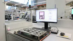
Siemens is collaborating with NVIDIA to increase engineering productivity, notably by boosting manufacturing yields of printed circuit boards (PCBs). Siemens’ Teamcenter software for product lifecycle management (PLM) and Process Preparation X and Siemens’ digital twin technology are being used with NVIDIA Cosmos to accelerate production planning.
Shorter manufacturing cycles are being achieved with the aid of automated optical inspection (AOI) powered by artificial intelligence (AI). By digital signal processing and analysis in the digital realm, electronic manufacturers can optimize product designs before starting a physical production process (see image above).
Quality control of manufactured electronic products is typically achieved with the help of optical inspection processes. Such processes are typically created by building and working with a physical product prototype. But by moving essential parts of the process, such as PCB design and formation of a bill of materials (BOM) for the PCB to a virtual world in the digital realm, a digital twin of the product prototype (rather than a physical board) can be created to provide insights into the types of preparation required for manufacturing that product.
A digital twin of an electronic product to be manufactured can be used with NVIDIA Cosmos to create an ideal prototype PCB layout. Images of PCB defects can also be created, by means of NVIDIA Cosmos Data Factory, to be used as warning signs to calibrate optical inspection systems.
This collaboration of digital tools for the sake of speeding electronic manufacturing processes is being demonstrated at the Siemens Electronics Factory in Erlangen, Germany. The location serves as a training ground and a starting point for customer education on advanced automated manufacturing processes powered by AI technology.
The factory provides a full-scale production environment and can be adapted to many scales and use cases to improve the manufacturing quality for a product of interest.
Learn more about digital twin technology
 dreamstime_m_464816680



About the Author
Jack Browne
Technical Contributor
Jack Browne, Technical Contributor, has worked in technical publishing for over 30 years. He managed the content and production of three technical journals while at the American Institute of Physics, including Medical Physics and the Journal of Vacuum Science & Technology. He has been a Publisher and Editor for Penton Media, started the firm’s Wireless Symposium & Exhibition trade show in 1993, and currently serves as Technical Contributor for that company's Microwaves & RF magazine. Browne, who holds a BS in Mathematics from City College of New York and BA degrees in English and Philosophy from Fordham University, is a member of the IEEE.



 Leaders Logo
Leaders relevant to this article: