Next-Gen Chiplet Interconnects Empower AI Systems
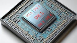
Sarcina Technology's new AI Platform offers patented methodologies for the UCIe-A (Universal Chiplet Interconnect Express-Advanced) and UCIe-S (Standard) protocols. These include an optimized RDL (redistribution layer) interposer design for die-to-die interconnections at data rates up to 32 gigatransfers per second (GT/s).
Optimizing the signal-routing architecture to minimize crosstalk and maximize signal integrity, chiplet-based architectures, and advanced package design delivers the performance required for next-generation AI systems.
Beyond the 32-GT/s die-to-die data rates compliant with UCIe 2.0 specifications, other features include maximized use of 3D space, with routing channels confined at the die edge for seamless integration of UCIe-A IP. Multidimensional routing optimizations for data, clock, and redundancy signals enable an ultra-compact 3D routing region, with a cost-efficient design that minimizes RDL routing layers, and standardized RDL layouts to improve fabrication yield.
The company's UCIe-S interconnect methodologies target organic substrates and advanced PCBs with high-density interconnect (HDI) technology, minimizing insertion loss and crosstalk to enable long channel lengths over standard organic substrates. The solution is compatible with package-to-package links over organic substrates or HDI PCBs, and is scalable to PCIe daughtercards, acceleration modules, and system baseboards.
Its 32-GT/s performance through advanced 3D high-frequency structure simulation (HFSS) paves the way for UCIe 3.0 adoption. The platform offers seamless die-to-die communication, even with silicon transmitter and receiver equalizations disabled, to eliminate extra transistor circuit power consumption.
In addition, Sarcina provides a design and simulation platform for chiplet interconnects across interposers, substrates, and PCBs, enabling the creation of partitioned monolithic SoCs into chiplets for higher yield and cost efficiency. It can also integrate heterogeneous technologies (compute, memory, analog, I/O) across process nodes, and incorporate silicon photonic dice and fiber array units (FAUs) with compute chiplets in a co-packaged optics package to eliminate data bottlenecks.
Related links:
New Product Highlights
About the Author

Alix Paultre
Editor-at-Large, Microwaves & RF
Alix is Editor-at-Large for Microwaves & RF.
An Army veteran, Alix Paultre was a signals intelligence soldier on the East/West German border in the early ‘80s, and eventually wound up helping launch and run a publication on consumer electronics for the U.S. military stationed in Europe. Alix first began in this industry in 1998 at Electronic Products magazine, and since then has worked for a variety of publications, most recently as Editor-in-Chief of Power Systems Design.
Alix currently lives in Wiesbaden, Germany.
