EM-Plugs: Speedy Simulation for Higher-Accuracy RF Digital Twins
What you'll learn:
- Traditional ways to characterize RF IC performance.
- What is EM-Plug simulation?
- A look at EM-plug model methodology.
- How EM-Plug leads to higher-accuracy RF digital twins.
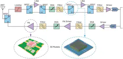
RF ICs are widely deployed across advanced applications such as 5G millimeter-wave (mmWave) systems, satellite communications, automotive radar, and high-end test and measurement platforms. Devices such as low-noise amplifiers (LNAs), power amplifiers (PAs), RF switches, digital step attenuators (DSAs), digitally tunable filters, and beamformers address these applications with solutions operating up to 90 GHz (Fig. 1).
When an RF IC is implemented on a substrate that differs from the vendor’s reference design, RF performance can deviate significantly, especially as the frequency ascends. Predicting this behavior isn’t straightforward, and traditional S-parameters can’t account for these variations.
Traditional Characterization of RF IC Performance
Optimizing the RF performance of the IC requires evaluating multiple chip-to-PCB transition options: RF trace type or layout- and process-sensitive parameters such as pad size and clearance, necking and tapering into 50-Ω transmission lines. Depending on design targets and manufacturing constraints, the transition may be realized as coplanar waveguide (CPW), microstrip, or stripline, while solder mask and solder paste profiles further influence the final RF response.
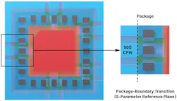
While S-parameters remain the standard method for characterizing RF performance metrics such as return loss, gain, and isolation, they’re defined at a reference plane typically located at the chip boundary or at the end of a 50-Ω trace (Fig. 2). This reference plane effectively freezes the chip-to-PCB transition for a substrate and assembly configuration where S-parameters are measured.
As a result, S-parameters can’t accurately predict how device performance will change when implemented on a different substrate, creating a blind spot in RF analysis. Neglecting these transition effects often leads to degraded return loss and signal-integrity issues.
To overcome this limitation, RF designers relied on fabricating standalone PCB test coupons or matrix boards that evaluate multiple transition and stackup combinations for a given device. While effective, this approach is both costly and time-consuming, as it requires manufacturing and measuring multiple boards.
The challenge is further compounded by advanced packaging technologies such as QFN and BGA. They introduce additional variables including solder-joint behavior and package-induced parasitics, increasing the complexity of accurately predicting system-level performance.
>>Download the PDF of this article
Another commonly used method involves full-wave electromagnetic (EM) simulation to analyze chip-to-PCB transitions for a given RF IC and target substrate. Full-wave EM simulation provides detailed insight into parasitic effects, coupling mechanisms, and radiation losses, enabling engineers to design transitions based on specific PCB stackups and iterate toward improved performance.
However, that approach typically requires access to a complete EM model of the IC, which can introduce intellectual-property (IP) constraints between organizations. In addition, full-wave simulations are computationally intensive, often requiring long run times, and make it impractical to explore manufacturing and assembly tolerances due to the large number of simulations required.
A New Approach: EM-Plug Simulation
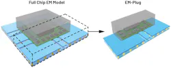
In response to these challenges, Analog Devices (ADI) developed the EM-Plug simulation tool (Fig. 3). In this approach, EM models of the package transition region are encapsulated and delivered directly to the user.
This lightweight, modular method is designed to optimize chip-to-PCB transitions for high-frequency RF products, making it possible to quickly evaluate critical PCB variables including:
- Landing-pattern geometry
- Substrate thickness
- Dielectric constant
- RF trace type
- Solder paste and mask profiles
- Chip placement or bond-wire configuration
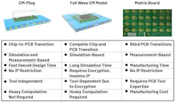
A single EM-Plug simulation is completed in minutes, compared to the multiple hours required for full-wave EM analysis. Figure 4 compares the EM-Plug approach with traditional full-wave EM simulation and matrix-board methods.
How Do EM-Plug Models Work?
An EM-Plug model encapsulates a localized section of the PCB that includes the RF transmission line segment, the chip-to-PCB transition, and relevant assembly details such as solder mask and solder paste. For chip-and-wire implementations, the EM-Plug tool instead models the chip pad geometry, bond-wire structure, and a small portion of the target substrate, such as alumina or low-temperature co-fired ceramics (LTCCs).
In both cases the EM-Plug tool focuses exclusively on the physical transition region that dominates high-frequency behavior.
Alongside the EM-Plug model, there’s an RF-core file in the form of an S-parameter dataset that represents only the internal characteristics of the RF IC. The RF core is intentionally decoupled from the package and PCB environment. It’s intended to be combined with the EM-Plug simulation results to form a complete representation of the device as implemented on the target board.
The development of 3D EM-Plug cores relies on a proprietary algorithm designed to ensure seamless integration and functionality. The approach is based on a combined analysis of the chip-to-PCB transition modeled in EM simulation and measurement-based representation of the device internals. This combination of EM-based transition modeling and measurement-based device characterization forms the foundation of the EM-Plug approach, enabling accurate and efficient RF IC representation in system-level simulations.
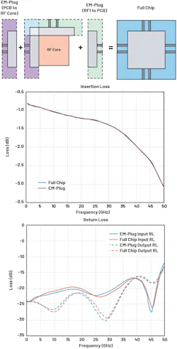
To model the full RF signal path, an EM-Plug model is generated for each RF pin of the component. These individual transition models are then combined with the RF core using standard S-parameter cascading techniques. Figure 5 illustrates this use, showing how the EM-Plug models and RF core collectively reconstruct the complete RF transition and device behavior within the customer’s system.
EM-Plug models are reference design assets made publicly available without IP restrictions. The models are compatible with standard commercial EM simulation tools — including ANSYS HFSS, Keysight ADS/EMPro, or any other similar software. Thus, engineers can integrate them easily into existing workflows and perform flexible, tool-independent optimization.
Figure 6 demonstrates EM-Plug-based results in comparison to a full-chip result. The EM-Plug approach accurately predicts the full-chip performance while completing the simulation within minutes, whereas the full-chip EM simulation requires approximately four hours on parallel computing resources.
EM-Plug Use Cases
RF Switch Integration on Alternative PCB Stackups
In real-world designs, system designers can’t replicate the exact evaluation board stackup due to component density, mechanical constraints, or manufacturing limitations. As a result, the RF transition must be re-optimized for an alternative substrate configuration.
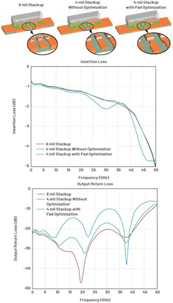
For example, consider a system using the ADRF5049 on an RO4003 substrate but constrained to a reduced thickness of 4 mil rather than the reference design of 8 mil. In this case, the CPW dimensions and pad geometry must be adjusted to compensate for the impedance change introduced by the thinner substrate.
Figure 7 compares three different chip-to-PCB transition implementations evaluated using the EM-Plug approach. All simulations were completed within minutes using ANSYS HFSS, enabling rapid exploration and optimization of the transition geometry.
RF Amplifier Performance Prediction Across Stackup Variations
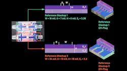
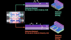
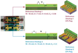
EM-Plug models can also be combined with measured data to extend the modeling approach beyond purely simulated environments. To demonstrate this capability, a coupon-based test structure was designed to evaluate performance across multiple PCB stackups. The ADL8102, a gallium-arsenide (GaAs) LNA in a lead-frame chip-scale package (LFCSP) operating up to 22 GHz, was selected for this study.
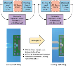
Two stackups were evaluated: Stackup 1 has an 8 mil thickness to ground plane, while Stackup 2 has an 18 mil total thickness to ground plane on different effective dielectric constants. These changes significantly affect transition behavior and CPW dimensions. Figure 8 shows the fabricated PCBs on the left, which include through-line structures for de-embedding purposes. On the right, the corresponding EM-Plug models are shown.
Using EM-Plug models, the RF performance of the ADL8102 on both stackups can be estimated. The predicted results show strong correlation with measured data (Fig. 9), validating the accuracy of the EM-Plug methodology for measurement-based workflows.

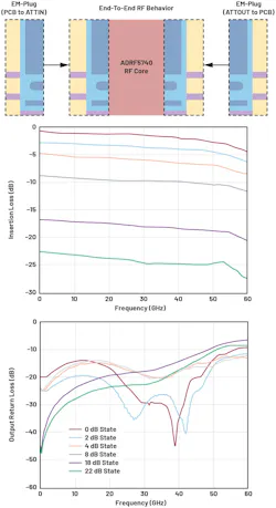
Devices with Multiple RF States: Digital Step Attenuators
The EM-Plug approach is particularly effective for RF ICs with multiple operating states, such as DSAs. For these devices, a single optimized EM-Plug model can be reused while cascading it with RF core models corresponding to different attenuation states. This enables efficient evaluation of RF performance across all operating modes without repeating EM simulations for each state.
Figure 10 shows EM-Plug-based simulation results for the ADRF5740 across multiple attenuation settings, demonstrating how state-dependent behavior can be analyzed rapidly and consistently.
Support for Multiple Package Types and Transmission-Line Implementations
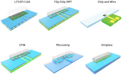
EM-Plug models are available for a wide range of RF IC package types and transmission-line structures. The approach supports common RF interconnect styles such as coplanar waveguide, microstrip, and stripline, as well as multiple package formats including LGA, LFCSP, chip and wire, and flip-chip surface-mount technology (SMT).
Figure 11 illustrates representative EM-Plug models for different package (top) and transition (bottom) configurations, highlighting the flexibility of the methodology across diverse RF integration scenarios.
Enabling Accurate RF Digital Twins
As RF ICs continue to operate at higher frequencies and become more tightly integrated into complex systems, accurately predicting real-world performance becomes increasingly challenging.
Traditional characterization methods centered around S-parameters are no longer sufficient to capture the impact of chip-to-PCB transitions, substrate variations, and assembly effects that ultimately define system behavior. This long-standing gap has limited the fidelity of RF simulations and increased reliance on hardware iterations.
EM-Plug models introduce a fundamentally new modeling approach by bringing the chip-to-PCB transition directly into the electromagnetic simulation domain in a practical and scalable way. By partitioning the problem into a transition-focused EM model and a core RF representation, EM-Plug models capture the dominant sources of performance variation without exposing sensitive IP or requiring computationally intensive full-chip EM simulations.
EM-Plug models also serve as a critical building block toward an accurate RF digital twin — one that reflects how a high-frequency RF component behaves in its actual system environment rather than under idealized assumptions. The approach is inherently applicable to a broad range of RF components and integration scenarios.
Looking ahead, the vision is to extend EM-Plug coverage across the entire high-frequency RF portfolio, enabling consistent, high-fidelity digital-twin representations that bridge characterization and real-world implementation.
>>Download the PDF of this article
About the Author
Sinan Alemdar
Product Applications Engineer, Analog Devices Inc.
Sinan Alemdar is a product applications engineer in ADI’s ADEF and Communications Group, working from the Istanbul Design Center. He provides application support for a range of RF products, including switches, attenuators, and front ends. He joined Analog Devices in 2016, after spending four years in the aerospace and defense industry. Sinan holds B.S., M.Sc., and Ph.D. degrees in electrical engineering from Bilkent University.
Gokhan Karaova
Product Applications Engineer, Analog Devices Inc.
Gokhan Karaova is a senior product applications engineer in ADI’s ADEF and Communications Group, working from the Istanbul Design Center. He provides application support for a range of RF products, including RF amplifiers, switches, attenuators, and front ends. He joined Analog Devices in 2022. Gokhan holds B.S. and M.Sc. degrees in electronics engineering from Middle East Technical University.
