Phase Sync in Digital Phased Arrays Through Direct RF Sampling (Part 1): The Basics
What you’ll learn:
- Radar synchronization relies on well-synchronized clocks.
- The wideband digitizer architecture and sync process.

Early antenna array systems deployed mechanical rotation systems to point the beam in the desired direction. With the advent of phased arrays, beamsteering has been accomplished electronically by applying phase offsets to individual antenna elements.
In an all-digital beamforming system, the RF signal from each antenna element is directly digitized by an analog-to-digital converter (ADC) and a digital-to-analog converter (DAC). These ADCs and DACs generally have sampling rates and usable analog bandwidths of up to a few gigahertz. This enables direct digitization of the L/S/C/X- and Ku-bands.
Scanning the entire volume of area with a single beam lowers the scan rate. A better approach is an element-level digital one that provides a faster scan rate and encompasses multiple beams in the area of interest. Each of these subarrays has individual gain and phase control for each element.
Unlike a hybrid or analog beamforming technique, each antenna element is digitized by a distinct channel of a high-speed data converter.1 Today’s high-speed converters have multiple integrated ADCs and DACs and hence offer greater channel density.
With technology advances in high-speed data converters (HSx), much of the digital-signal-processing (DSP) functionality is now embedded into a single integrated circuit (IC).2 This relaxes the resource and power consumption on the field-programmable gate array (FPGA) used in the subarray module.
DSP components, such as decimation and interpolation blocks, allow for low baseband sampling rates (a few tens of megahertz to a few gigahertz) and a high final sampling rate (a few gigahertz). Thus, the FPGA can operate at lower sampling rates.
Integrated numerically controlled oscillators (NCOs) will allow for frequency upconversion and downconversion through the IC itself. The usage of such ICs guarantees good noise performance3 as well as simplification of the RF signal chain, as it eliminates the need for multiple stages of frequency upconversion and downconversion.
Large all-element digital phased arrays depend on the phase relationship between all channels. Consequently, the entire radar system depends on a calibration that establishes a known phase offset between the channels. The RF channels will emanate from different high-speed converter ICs housed on different boards.
In this article, we propose a method to ease the system-level calibration by achieving a known phase relationship between the channels of multiple Analog Devices AD9081 RF DAC/ADCs, thus allowing a lookup table (LUT)4 to be populated with these precalibrated phase values.
The degree of repeatability has been demonstrated through oscilloscope statistics in the following sections.
Clock Generation, Distribution, and Synchronization
If radar systems are to achieve synchronization, they rely on how well clocks are synchronized. In addition, multiple boards must receive a reference from the same reference source, which requires synthesis of a clock tree. This work involves the use of the Analog Devices HMC7044 jitter attenuator on the AD9081 evaluation boards and the AD-SYNCHRONA14-EBZ multichannel system clocking device, which also has the HMC7044 inside the module.
The HMC7044 is a clock generator and distribution IC that has a dual phase-locked-loop (PLL) architecture (Fig. 1). The first PLL (PLL1) acts as a jitter cleaner, meaning it allows a noisy reference to lock to a cleaner voltage-controlled crystal oscillator that sits locally on the individual boards.
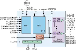
In this scenario, the AD-SYNCHRONA14-EBZ distributes references to the AD9081 evaluation boards. The loop filter of PLL1 typically has a very narrow bandwidth, making it possible for the cleaner VCXO that sits locally on the board to dominate the clock noise performance at lower offsets.
Thanks to its 14 clock outputs, the HMC7044 distributes device clocks to the wideband digitizers as well as the necessary FPGA and system references (SYSREFs). Each of the 14 outputs has individual delay controls that help align clocks by compensating for any phase discrepancies arising due to trace mismatches.
Synchronization between these 14 outputs can be carried out by a Serial Peripheral Interface (SPI)-based reseed command, but because this use case involves syncing multiple such ICs, we use the SYNC pin to distribute an aligned synchronization pulse to the HMC7044s. In a successful capture of this sync pulse, the outputs of multiple clock-distribution ICs should be aligned to each other. The clock-tree setup with the AD9081 evaluation boards and the AD-SYNCHRONA14-EBZ will be described in Part 2 of this series.
An Overview of the Wideband Digitizer Architecture and Sync Process
This work aims to achieve a repeatable phase offset between multiple AD9081s that fall under the family of high-speed digitizers. An immense amount of DSP is embedded within the digitizer (Fig. 2). The ADCs and DACs within the digitizer can sample at maximum rates of 4 and 12 GSPS, respectively.
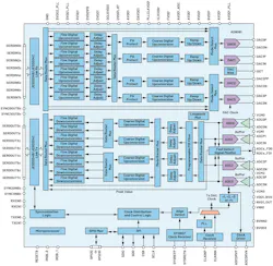
Programmable filters (PFILTs) are integrated along the receive path, where the user can program custom coefficients to implement a digital finite-impulse-response (FIR) filter. The digital upconverters (DUCs) and downconverters (DDCs) help with dividing or multiplying the data rates to and from the FPGA. The DDC and DUC blocks also include the NCOs for frequency translation.
The analog ADC supports a bandwidth of up to 8 GHz. The baseband interface is over the standard JESD (JEDEC Electrical Standard for Data) protocol, and both JESD204B and JESD204C versions are supported.
The MxFE wideband, mixed-signal front-end family provides the option to either feed the high-frequency sampling clock (12 GHz) directly or supply a low-frequency clock of a few hundred megahertz and use the internal PLL to generate the 12-GHz sampling clock. Here, we have implemented the latter. The clock-receiver pins remain the same, and the user can control the mode of clocking through the application programming interface (API) in the firmware.
The DSP blocks relevant to the approach described here are the internal PLL, the NCOs, and the sync logic. The sync logic works in two steps. The first is the one-shot sync that aligns the baseband clocks and other clocks within the IC; the second consists of the alignment of the NCOs for the different digitizers. The one-shot sync depends on the capture of an externally fed SYSREF clock signal.
For our purpose, we used a continuous SYSREF signal, but there’s support for an N-pulse and a gapped periodic signal. The one-shot sync aligns the internal local multi-frame clock (LMFC)/local extended multi-block clock (LEMC) to the external continuous SYSREF signal. The AD9081 provides a register that can be read back to confirm the completion of the one-shot sync.5
In the case of an AD9081, once the bit describing the status of the one-shot sync is read back as high, we can measure the phase offset of the LMFC and the external continuous SYSREF to determine how well they’re aligned. To facilitate this, the digitizer IC features a register that stores the phase offset between the LMFC and the SYSREF in units of DAC sampling clock cycles. Here, the DAC sampling clock was set to 12 GHz.
A zero read back from the phase registers implies that the LMFC is indeed aligned to the SYSREF signal coming from the clock distribution IC, the core of the clocking system on the AD9081 development boards.
The second step is to align the NCOs. This step can be understood as the synchronization of local oscillators (LOs) in the analog RF domain. There are two ways to do this: resetting the NCOs directly with an external SYSREF signal or using a general-purpose input/output (GPIO)-based system.
In this case, we used the leader-follower-based sync. One of the boards acts as the leader that triggers the synchronization on both the leader and the follower boards and uses a GPIO for alignment between platforms. There’s a firmware and hardware-description-language (HDL) dependency to make this happen, which will be described in detail in Part 2. The API prepares both the digitizers for triggering the NCO sync and the NCOs reset at the same time on the next rising edge of the LMFC on both the boards.
The one-shot sync, followed by the leader-follower NCO sync, forms the basis of syncing multiple digitizers. In addition, the NCOs allow for phase control within the range of –180° to +180°, and this is exposed through the APIs.
For more flexibility, the digitizer offers multiple options to initiate the NCO reset after a specific GPIO is captured: the external SYSREF signal, the LMFC rising edge, or the LMFC falling edge. The API is configured to reset the NCOs at the next LMFC rising edge after the GPIO pin is driven high by default, but we use the SYSREF signal for triggering the reset action.
The method of NCO sync we’ve described applies when the GPIO pins of the leader and follower boards can be connected. If this isn’t possible, we also evaluated another method whereby all of the boards are set as followers, and the baseband logic device issues a GPIO-high on both the digitizers.
During the initial phases of the project, the codes were made to wait for keyboard inputs to allow for the GPIOs triggering the reset to be set manually. Once we proved that the concept works, this was automated through the HDL and firmware, waiting for the GPIOs to be triggered.
Because the clocks being fed to the digitizer IC also need to have a repeatable phase relationship, there’s also a need to sync the clock-distribution ICs on both the leader and follower boards that generate the SYSREF signals and the device clocks for the digitizers. The clock-distribution ICs have been synced through a complementary metal-oxide semiconductor (CMOS) pulse into the SYNC pins.
In the setup, the AD-SYNCHRONA14-EBZ clock controller generates phase-aligned references and CMOS sync pulses to the HMC7044s on the leader and follower AD9081 evaluation boards.
The methodologies described in the previous section also remain applicable if the AD9081s are on the same board.
Part 2 will discuss the procedure with the API codebase for the AD9081, HMC7044, and the FPGA HDL. It also will present the actual hardware implementation and the results of phase repeatability, which have been achieved between the two AD9081 evaluation boards.
References
- Connor Pope, Hong Tang, Bowen Zheng, and Hualiang Zhang. “Phased Array Systems—Design Considerations and System Demonstration.” 2024 IEEE International Symposium on Phased Array Systems and Technology (ARRAY), October 2024.
- W. Michael Jones, Stephen Pancrazio, Bryce Readyhough, and John Majewski. “A 0.1-20 GHz Digitizer SOM Useful for Phased Array Applications in a Standardized Form Factor.” 2024 IEEE International Symposium on Phased Array Systems and Technology (ARRAY), October 2024.
- Caleb Fulton, Mark Yeary, Daniel Thompson, John Lake, and Adam Mitchell. “Digital Phased Arrays: Challenges and Opportunities.” Proceedings of the IEEE, Vol. 104, 2016.
- Michael Jones, Michael Hennerich, and Peter Delos. “Power-Up Phase Determinism Using Multichip Synchronization Features in Integrated Wideband DACs and ADCs.” Analog Devices, Inc., October 2020.
- System Development User Guide for the AD9081 and AD9082 Direct RF Sampling Transceivers. Analog Devices, Inc., May 2023.
>>Download the PDF of this article

About the Author
Archishman Guha
Applications Engineer, Analog Devices Inc.
Archishman Guha received his M.Tech. in space engineering from the Indian Institute of Technology, Indore, India. He is an applications engineer at Analog Devices, focusing on the aerospace and defense sector. His areas of focus include high-speed data converters, clocks, and PLL applications.
George Mois
Embedded Systems Architect, Analog Devices Inc.
George Mois has been with Analog Devices since 2021. He works on bare-metal and Linux kernel drivers for ADI parts, especially transceivers. He holds a Ph.D. in systems engineering from the Technical University of Cluj-Napoca, Romania, where he also teaches embedded systems classes.