Solderless Processes Enhance the Five Pillars of High-Performance Microwave and RF Circuits
What you’ll learn:
- Conventional solder-based PCB assemblies introduce parasitic inductance and capacitance and impedance discontinuities.
- Solderless assembly processes invert traditional PCB construction by encapsulating components first and then forming copper interconnects directly onto their terminals.
- The method can improve reliability and performance of RF systems in harsh environments.
The evolution of microwave and RF systems is being driven by demands for higher bandwidth, lower latency, improved power efficiency, and operation in increasingly constrained and hostile environments. While semiconductor technologies like GaN, SiGe, and advanced CMOS enabled dramatic gains in device performance, the interconnect structures that link these devices into functional systems haven’t advanced at the same pace.
In fact, at microwave and mmWave frequencies, the interconnect often becomes the dominant limiter of system performance. Against this backdrop, solderless assembly processes using direct copper interconnection to component terminals (such as the Occam process) represent a fundamentally different approach that may be well-suited to RF and microwave applications going forward.
A Brief Description of Solderless Assembly
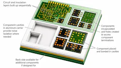
At its core, this approach inverts the conventional printed-circuit-board (PCB) paradigm. Rather than fabricating a board and then attaching components via solder, components are first placed and encapsulated, and copper interconnects are subsequently formed directly onto their terminals (see figure).
Such a process eliminates solder joints and leads to a more integrated, fabrication-like method of system construction. While broadly applicable across electronics, the advantages of the proposed method appear to be especially compelling in the RF domain, where electrical parasitic effects, electrical/signal discontinuities, and thermal constraints are critical determinants of device and system performance.
Among the most sought-after and desirable improvements in RF circuits lies in the reduction of parasitic inductance and capacitance.
In conventional surface-mount technology (SMT), even carefully designed interconnects introduce discontinuities due to the nonuniformity of solder joints, varying pad geometries, and via transitions. At microwave frequencies, these discontinuities, largely unregistered in traditional circuits, can significantly degrade impedance matching, increase insertion loss, and introduce unwanted reflections.
Forming copper interconnects directly onto component terminals using fine-line build-up processes as proposed can shorten signal paths and minimize interfaces. The result is improved impedance continuity and reduced signal degradation, which is essential for high-frequency performance.
Solderless Assembly Brings Signal Integrity Benefits
Closely related is the improvement in general signal integrity. RF systems rely on tightly controlled transmission-line structures. These include such instantiations as microstrip and stripline constructions, and coplanar waveguides, where geometry and dielectric properties must be precisely managed.
A solderless, build-up interconnect approach, leveraging techniques like methods used in advanced semiconductor packaging, allows for finer feature sizes and tighter tolerances than that provided by conventional PCB fabrication. Transmission lines can be integrated directly into the structure with greater precision, while the elimination of solder joints removes a source of variability and impedance discontinuity. This contributes to more predictable and repeatable electrical behavior across production units.
Another important advantage of the proposed method is the potential for three-dimensional (3D) integration. RF systems increasingly benefit from compact, multilayer architectures where active and passive components are closely co-located.
In traditional designs, achieving this requires complex multilayer PCBs with numerous vias and interconnect transitions, each introducing loss and reliability concerns that must be monitored. However, by embedding components within a dielectric matrix and routing copper interconnects around them, a solderless architecture enables more efficient use of volume. As a result, we can shorten interconnect lengths, minimize vertical transitions, and boost system density.
For applications such as phased-array antennas, compact radar modules, and high-frequency communication systems, these improvements translate directly into enhanced performance and reduced size and weight.
Solderless Assembly Aids Thermal Management
Thermal management is another area where direct copper interconnection provides meaningful benefits. RF and microwave devices — particularly high-power amplifiers based on gallium nitride (GaN) or laterally diffused metal-oxide semiconductor (LDMOS) technologies — generate significant heat that must be efficiently dissipated.
In conventional assemblies, thermal paths are often indirect, relying on solder joints, thermal vias, and external heatsinks. A solderless approach allows thermal-management features, such as embedded copper planes or heat spreaders, to be placed directly or integrated in proximity to active devices.
Because electrical and thermal paths can be designed concurrently, rather than sequentially, it’s possible to achieve lower thermal resistance and more uniform temperature distribution across the module. In other words, thermal problems are able to be dealt with at the front end of the design process rather than at the back end, as is often the case (see figure, again).
Reliability, which is especially a concern in the case of RF systems deployed in harsh environments, can be enhanced by eliminating solder. Solder joints are a well-known source of failure due to thermal cycling, mechanical stress, and material fatigue. In high-frequency systems used in aerospace, defense, and automotive radar, these stresses can be particularly severe.
Replacing solder joints with direct copper interconnections removes a primary failure mechanism, potentially extending system lifetime. In addition, the lower processing temperatures associated with solderless assembly reduce thermal stress on sensitive RF components during manufacturing.
A Path Toward Module-Level Integration in RF Systems
This approach also aligns well with the growing trend toward module-level integration in RF systems. Rather than assembling discrete components onto a large board, many modern designs favor highly integrated modules that can be treated as functional building blocks.
Solderless, direct-interconnect techniques enable the creation of compact RF modules that integrate active devices, passives, and interconnects into a single structure. These modules can then be incorporated into larger systems using conventional attachment methods where necessary, preserving flexibility while capturing the performance benefits of the embedded architecture.
Despite the advantages described, adoption of such a promising process will not be immediate or universal. Challenges remain — lessons need to be learned in process control, yield management, and ecosystem development. RF components often have specialized packaging and material requirements, and ensuring compatibility with embedding and direct interconnect processes will require careful engineering.
Using the process in rework is an option for correcting problems with design and manufacturing. This has sparked concerns as to the reworkability of such embedded assemblies. It’s believed that placing a greater emphasis on the use of known-good components, careful manufacturing, and robust in-process inspection can ameliorate worries, but it will require a change of long-held status quo mindsets.
That said, the apparent trajectory of RF and microwave technology suggests that the limitations of conventional solder-based assembly will become increasingly constraining. As operating frequencies extend into the mmWave and sub-terahertz regimes, even small interconnect imperfections can have outsized effects. In this context, solderless assembly using direct copper interconnection offers a compelling alternative — one that treats interconnects as an integral part of system fabrication rather than a secondary step.
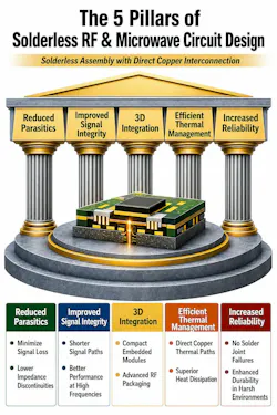
In summary, replacing solder-based assembly with direct copper interconnection, as suggested and promoted by the Occam process, has the potential to significantly enhance the manufacture of microwave and RF circuits. It will do so by providing five pillars of improvement (see figure, again):
- Reducing electrical parasitic effects
- Improving signal integrity
- Enabling 3D integration
- Enhancing thermal management
- Increasing reliability
This approach aligns closely with the evolving demands of high-frequency systems. While initial adoption is likely to occur in certain high-performance and high-reliability applications, the underlying principles suggest a broader role in shaping the next generation of RF electronics.
>>Download the PDF of this article
About the Author
 Joe Fjelstad
Joe Fjelstad
Chief Technology Officer, The Occam Group
Joseph Fjelstad has been active in electronics manufacturing since 1972 in roles including chemist, process engineer, and R&D manager. He holds nearly 190 U.S. patents and numerous foreign ones, and is an internationally recognized expert, inventor, and lecturer in electronics interconnection technology. Fjelstad is also a veteran of several startup companies, including Beta Phase, ELF Technologies, MetaRAM, Silicon Pipe, and Tessera (now Adeia).
Many of Fjelstad’s innovative devices and reliability-enhancing IC packaging features are found in nearly every electronic device made today. He’s also the author, co-author, or editor of several books on interconnection technology, including Flexible Circuit Technology, 4th Edition, Chip Scale Packaging for Modern Electronics, and Solderless Assembly For Electronics—The SAFE Approach (the Occam Process). Over the past five decades, he has written hundreds of articles, columns, and commentaries for industry magazines and journals.
Related
 Leaders Logo
Leaders relevant to this article: