
Components based on gallium nitride (GaN) offer a range of important benefits versus silicon devices, including smaller size allowing for greater power-density circuits, improved efficiency, reduced switching losses, better power handling, and several other performance attributes. These factors are critical to meeting the increasingly demanding high-power, high-density needs of today’s designs in applications ranging from USB Type-C/PD-enabled consumer products like adapters to telecom and industrial applications.
However, myths about GaN have emerged, too. Let’s take a closer look.
1. GaN is all about high-frequency operation, primarily to reduce the size of the passive components.
GaN HEMTs (high-electron-mobility transistors) have excellent RDS(on) * Qg figure of merit (FOM). Depending on the voltage and current rating, FOM can be somewhere between 4X to 10X lower than that of a superjunction (SJ) FET. Therefore, GaN is suitable for high frequency of operation. Most of the early adopters of GaN have focused on high-frequency operation and hence reduction in the size of the passive components. Some passive components especially magnetic technology hasn’t evolved as much as semiconductor technology thereby making the proliferation of GaN difficult.
An often-ignored area is the advantage that a better FOM brings at traditional frequencies of operation. Utilizing a lower-RDS(on) GaN HEMT can reduce the conduction losses and push the efficiency up. Often, this incremental increase in efficiency, coupled with innovative packaging, is all one needs to push the power-density curve up in the short to medium term.
2. There’s no play for GaN at low-frequency operation.
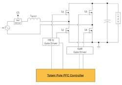
For the reasons mentioned above, GaN is often portrayed to benefit only at high frequency. However, topologies such as totem-pole PFC (TPFC), in which there’s no body diode and hence no reverse-recovery effect, bring a tremendous advantage (Fig. 1). In fact, this feature of GaN enables the TPFC to operate in continuous-conduction mode, which wasn’t previously possible. The TPFC topology can be run at frequencies <150 kHz and could result in efficiency gain of 1 to 2% in a 500-W PFC by eliminating the diode bridge. This improvement in efficiency and elimination of the bridge diode, along with its corresponding heatsinks, enables higher power density even at low-frequency operation.
3. GaN is expensive.
The notion that GaN is expensive stems from the initial price being quoted by various semiconductor vendors. GaN HEMT can realize the same RDS(on) as a SJ FET in less than half the size, resulting in more die per wafer. Once the initial startup costs are recouped, GaN will be cheaper than a SJ FET.
4. GaN will be first commercialized in a high-end niche application.
This is yet another myth propagated by the initial mistake of chasing extremely high-frequency operation. GaN has started to make inroads especially into the USB Type -C/PD and other consumer applications that are high volume but not very high reliability or critical like automotive applications.
5. The GaN ecosystem is still nascent.
This GaN ecosystem is evolving. Almost all of the semiconductor vendors are offering or plan to offer enhancement-mode GaN (eGaN) gate drivers or gate driver plus GaN HEMT in one package. For instance, there’s a complete ecosystem today that implements a TPFC, and it didn’t exist a few years ago.
6. GaN’s gate voltage needs to be tightly controlled.
First-generation eGaN HEMTs needed tight control of gate voltage and suffered long-term degradation or worse blowups in the product validation phase if the gate saw some voltage transients. But the latest-generation GaN HEMTs can handle larger gate voltage transients for a short period of time during turn-on phase, simplifying gate-driver design and layout.
7. GaN drivers need to always handle extreme dv/dt.
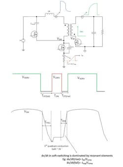
A persistent myth among the semiconductor companies is that GaN half-bridge drivers need to handle extreme dv/dt on the order of 200 V/ns, since the parasitic capacitances of the GaN HEMT is low. In fact, in most resonant topologies that achieve zero voltage switching (ZVS), resonance is primarily dictated by the transformer characteristics and the lump capacitances on the switch node (Fig. 2). Even while operating at high frequency, the dv/dt rarely if at all crosses 100 V/ns.
8. Third-quadrant operation can be prevented by paralleling a diode.
The voltage drop while GaN is conducting in the third quadrant (also called reverse conduction from source to drain) is on the order of −2 to −4 V, depending on the device and bias conditions. Hence, many engineers assume that paralleling an external diode can improve the efficiency. Often, this isn’t possible—GaN conducts very fast and the parasitic inductance present in the diode package makes it impossible for the current to steer through it.
9. Negative turn-off voltage is a must for eGaN.
While negative turn-off voltage can protect the eGaN from inadvertently turning back on during transients, it’s not necessary, especially if the layout follows all of the standard protocols. In fact, many of the eGaN gate drivers available in the market don’t feature negative turn-off voltage as it adds cost and complexity.
10. It isn’t possible to have dv/dt control of GaN devices.
This myth stemmed from the days of cascoded GaN HEMTs, where it wasn’t easily possible to control the turn-on and turn-off speed. eGaN behaves similarly to a SJ FET. Gate-drive circuitry can be tuned to control dv/dt.
11. All new wide-bandgap (WBG) materials work similarly.
GaN and silicon carbide (SiC) are both wide-bandgap materials. They are exciting for multiple reasons, but their characteristics, application space, and gate drive requirements are different. SiC will compete with IGBTs in the high-power space and very-high-voltage space (≥ 650 V). Meanwhile, eGaN will compete with SJ FET at all power levels from 40 to 650 V.
Ajay Hari is Applications Manager at ON Semiconductor.
About the Author
Ajay Hari
Applications Director, onsemi
Ajay Hari is an Applications Director at onsemi where he’s responsible for leading a team of product definers and applications engineers for ac-ac and isolated ac-dc power management. Prior to onsemi, Ajay worked at National Semiconductor/TI, specializing in isolated power converters. He’s defined many PWM ICs for telecom, automotive, and industrial markets.
Ajay started his career at General Electric Lighting as a design engineer. He’s published numerous technical papers and has over 10 patents issued/ongoing. Ajay is an active participant in PSMA and is co-editor of the PSMA applications section roadmap. He holds a Master of Science in Electrical and Computer Engineering from the University of Florida.
