A Deep Dive into the Quad-Apollo MxFE X-Band Beamforming Platform
What you'll learn:
- How four AD9084 Apollo MxFE converters can be synchronized for 16Tx/16Rx X-band beamforming.
- How the RF front end uses tunable filters, LNAs, DSAs, and bypass paths to balance linearity and bandwidth.
- How JESD204C clocking and synchronization maintain deterministic latency and phase coherence across channels.
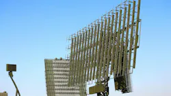
The Quad-Apollo MxFE (mixed-signal front-end) X-band direct sampling digital beamforming platform is an advanced, every-element digital, direct RF-sampling solution that serves as a complete reference architecture for next-generation digital beamforming systems (Fig. 1).
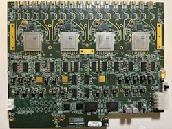
Designed to highlight the capabilities of Analog Devices’ MxFE technology, the platform integrates all critical subsystems — RF signal conditioning, precision clocking, multichip synchronization, and DC power management — into a unified environment that supports coherent, scalable signal processing across multiple channels.
Each subarray within the platform comprises 16 receive and 16 transmit channels configured in a uniform linear array, with an element spacing corresponding to half a wavelength at 12 GHz. This geometry optimizes spatial sampling for X-band operation while supporting full digital beamforming across all elements. The platform demonstrates how multiple AD9084 Apollo MxFE data converters can be synchronized and clocked together within one coherent architecture, providing a realistic example of system-level integration for high-channel-count RF applications.
Beyond its role as a reference design,1 the Quad-Apollo MxFE platform serves as a development and evaluation tool for advanced radar and communications systems. Its architecture supports multiple simultaneous beams, adaptive nulling, and reconfigurable beam patterns, offering the flexibility required for modern phased-array radar, electronic warfare, and multimission sensing applications.
The system’s deterministic timing framework, broadband front end, and scalable synchronization scheme present a complete signal chain — from RF input to digital beamformed output — designed to accelerate innovation in high-speed, every-element digital array technology.
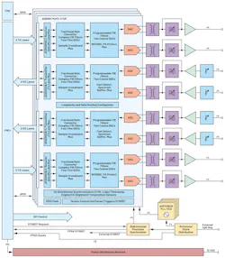
The block diagram in Figure 2 illustrates a single subarray’s transmit and receive RF front-end signal chain, the data converter equipped with hardened digital-signal-processing (DSP) features, multichip clocking solution, and 12-V DC power solution. A commercial off-the-shelf FPGA carrier card in combination with open-source low-level software drivers and MATLAB tool boxes enables software control of the system platform.2,3
RF Front End
The RF front end of the Quad-Apollo MxFE system is designed with intentional simplicity and modularity, emphasizing flexibility, performance, and ease of customization for a wide range of applications. As shown in Figures 3 and 4, the architecture leverages broadband, low complexity signal paths to ensure wide frequency coverage while maintaining high linearity and signal integrity throughout the chain.
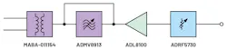
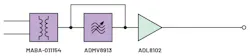
At its core, the design employs 2:1 broadband baluns to interface the high-speed ADCs and DACs with the remainder of the analog signal chain. Each transmit-receive channel incorporates a shared, digitally tunable X-band filter (ADMV8913), which provides precise frequency selection and out-of-band rejection.
This filter stage includes a board-level bypass path that can be activated through a capacitor rotation mechanism, allowing for direct sampling at S-, C-, and Ku-band frequencies. When the filter is bypassed, the system sacrifices the inherent anti-aliasing benefits provided by the ADMV8913, but it gains extended frequency flexibility for broadband or wideband applications where filtering can be handled digitally.
On the receive side, each channel features a highly linear broadband low-noise amplifier (LNA) followed by a wideband digital step attenuator (DSA) at the input stage. The DSA enables fine-grained analog gain control across varying signal conditions and is directly controlled via the data converter’s general-purpose input/output (GPIO) interface for rapid, deterministic adjustment during system operation. This architecture supports fast reconfiguration, suiting it for adaptive or real-time beamforming systems.
Receiver linearity is emphasized in the design, as intermodulation distortion products tend to be spatially correlated across elements in a fully digital, every-element phased-array system. By prioritizing linearity, Quad-Apollo MxFE technology ensures that dynamic range and spectral purity are maintained, even in multichannel coherent configurations.
For applications requiring additional frequency translation, gain stages, or specialized signal conditioning, the platform supports the integration of plug-in personality cards ahead of the front end. Such modular extension capability allows system designers to tailor the performance envelope to meet specific end-use requirements, whether optimizing for bandwidth, noise figure, or frequency coverage.
By keeping the subarray-level signal chain streamlined and broadband, the Quad-Apollo MxFE system provides a robust and flexible foundation for scalable, high-performance RF system development.
Clocking Architecture
Clocking plays a pivotal role in modern multiconverter systems, acting as the backbone that enables multichip synchronization, deterministic latency, and coherent signal combining across large, distributed architectures. Precise clock distribution helps ensure that every data converter, FPGA, and analog front end operates in harmony — an essential requirement for applications such as phased-array radar, high-channel-count instrumentation, and advanced communications systems.
In these systems, synchronization based on the JESD204C standard is achieved through a combination of dedicated clock-generation and clock-distribution blocks, supplemented by a bidirectional subclass 1 synchronizer. This architecture guarantees deterministic latency across all JESD204C channels, making it possible for system designers to predict and control timing at a nanosecond level. Furthermore, the synchronization scheme can be extended beyond a single subsystem, maintaining deterministic latency across multiple subarrays for large-scale implementations.
Figure 5 shows that a single high-stability reference clock serves as the foundation for the entire timing network. This reference is distributed through ultra-low jitter clock fanout buffers that feed the MxFE devices with clean, ultra-low phase-noise sampling clocks. Each MxFE device employs a dedicated two-wire clock interface that continuously maintains phase and frequency alignment, compensating for drift due to temperature changes or long-term aging effects.
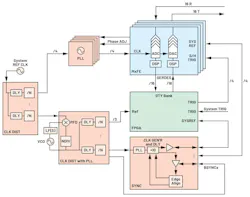
The same master reference also drives a secondary clock generation stage responsible for producing digital clocks for the FPGA fabric and providing precision reference signals to the synchronizer. A 10-channel precision synchronizer forms the heart of the coordination mechanism, delivering bidirectional, low-frequency timing signals that align all data converters and the FPGA to a common timing reference.
The synchronizer also enables per-channel propagation delay trimming. Thus, engineers can fine-tune alignment and phase relationships between channels for optimized performance.
Depending on the overall array architecture, the synchronizer can be deployed in daisy-chain or fanout configurations, ensuring scalable synchronization across multiple subarrays or system partitions. Even when operating at extremely high sample rates — up to 20 GSPS — the clocking infrastructure maintains deterministic alignment, ensuring phase coherence and timing integrity throughout the system.
By combining low-jitter clocking, hierarchical distribution, and JESD204C subclass 1 synchronization, the entire multiconverter platform achieves a unified, phase-stable timing framework that underpins high-speed data-acquisition and signal-processing performance.
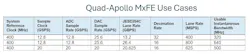
The table summarizes three representative operating configurations of the Quad-Apollo MxFE system driven by a 400-MHz reference clock. Together, these configurations illustrate the tradeoffs between sampling rate, digital decimation, and data throughput in optimizing bandwidth and interface performance for different system requirements.
Conclusion
System-level validation of the Quad-Apollo MxFE X-band digital beamforming platform confirms coherent operation across all channels, achieving sub-degree phase alignment and sub-picosecond timing accuracy. The demonstrated performance in adaptive beamsteering, spatial nulling, and multibeam transmission highlights the platform’s readiness to emulate next-generation radar and electronic-warfare architectures.
References
1. ADXBAND16EBZ Prototyping Platform User Guide, Analog Devices Wiki.
2. AMD Virtex™ UltraScale+™ FPGA VCU118 Evaluation Kit, AMD.
3. analogdevicesinc/HighSpeedConverterToolbox: MATLAB Toolbox for ADI High Speed Converter Products, GitHub.
About the Author
Siddhartha Das
System Applications Engineer, Analog Devices Inc.
Siddhartha Das is a systems applications engineer on the Subsystems and Sensors Team within Analog Devices’ Aerospace, Defense, and Communications Business Unit based in Durham, N.C. He earned his B.S. in electrical engineering from Virginia Tech in 2023 and is currently pursuing his M.S. in electrical engineering from the same institution.
Related
 Leaders Logo
Leaders relevant to this article: