Defining Transistor Load Impedances for Optimum, “Anti-Fragile” RF Amplifier Performance
What you'll learn:
- How to define the optimum fundamental and second- and third-harmonic load impedances for RF/microwave power amplifiers.
- Step-by-step procedure for transistor models with intrinsic generator access.
- The impact of transistor output.
When designing RF/microwave power amplifiers working under nonlinear operation, defining the fundamental-frequency load impedance, without ignoring the second- and third-harmonic load impedances, is critical for achieving optimal, robust, or even “anti-fragile”1 performance. Although numerous scholarly resources describe methods for determining these impedances for waveform-shaping modes like Class B, Class F, Class-inverse F, Class J, and their broadband derivatives, such methods often rely on complex mathematical expressions. These approaches can be challenging for engineers without advanced degrees.
This article presents straightforward procedures to define these impedances for optimal performance and robustness against tolerances, using accessible tools and nonlinear transistor models.
Many RF/microwave transistor datasheets provide load-pull Smith Chart data, but they often omit details about loads for the second- and third- harmonic loads or the rationale for their selection. A comprehensive nonlinear model and a simple procedure can provide accurate initial values for these impedances, enabling load-pull simulations for power, efficiency, and linearity.
Notably, some transistor models lack access to the intrinsic generator nodes, limiting waveform optimization. Nevertheless, an alternative and simpler procedure can be employed to help the design process in this situation.
For this work, Cadence/AWR’s Microwave Office is used for schematics and simulations. However, similar setups can be implemented in other simulators such as Keysight’s Advanced Design System (ADS).
Procedure for Transistor Models with Intrinsic Generator Access
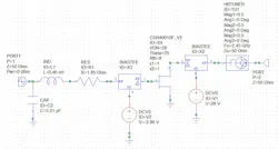
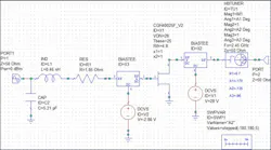
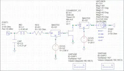
Step 1: Create an initial schematic (Fig. 1):
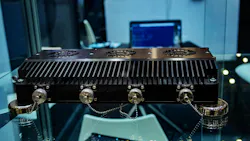
- Include your chosen transistor. In this case it’s a 25-W GaN HEMT device.
- Use an output tuner for the fundamental and the second- and third-harmonics frequencies with default values.
- Bias the drain current as indicated by the chosen transistor’s datasheet.
- Define a single frequency of interest in the simulator’s options/settings and for the tuner. In this case, the frequency of interest is 2.45 GHz.
- Use resistors, inductors, and capacitors to tune the input using linear simulation for a good input match and K factor of ≥1 to minimize the input power and distortion of input nonlinear effects at the output.
Step 2: Single-tone harmonic balance setting
- Configure the harmonic balance simulation to use one tone, producing a pure sinusoidal output at the fundamental frequency. This effectively shorts all harmonics across the intrinsic generator nodes.
Step 3: Tune the fundamental-frequency loadline for maximum power
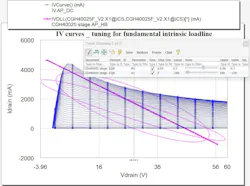
- With appropriate input power, adjust the output tuner’s reflection coefficient (amplitude and angle) at the fundamental frequency to maximize output power. Simultaneously, plot the loadline over the transistor’s IV curves at the intrinsic generator (Fig. 2).
- Note that the loadline, finely tuned for maximum power, is a straight line as the laws of physics dictate. It represents how the load impedance at the output node of the transistor model provides maximum voltage and current swing at full saturation for the output power with the parasitic elements of the intrinsic generator’s reactances tuned (or resonated) out.
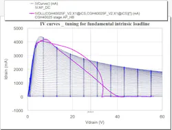
- Understand that the loadline at the fundamental frequency, being a sinusoid tone, isn’t contained by the IV curves of the transistor. A harmonic-balanced simulation with 15 tones (Fig. 3) is the complex loadline, and it’s confined inside the IV curves.
Step 4: Three-tone simulation and Class B tuning
- Switch to three tones for the harmonic-balanced simulations.
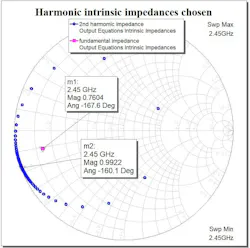
- Simulate and plot the intrinsic fundamental and second/third-harmonic-reflection coefficients (impedances) on a Smith chart.
- As expected, the fundamental intrinsic impedance is on the central line, where the pure resistance impedances are found (Fig. 4).
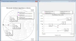
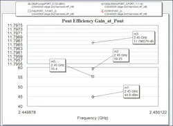
- Tune the second- and third-harmonic-reflection coefficients to be with magnitude of 1 and angle at the point of ±180°, i.e., at the point of short circuit (Fig. 4, again).
- This is a classic Class B mode of operation. The right side of Figure 4 plots the gain at Pout at Pout¸ power-added efficiency (PAE), and drain efficiency at an input power of 33 dBm.
Step 5: Sweep harmonic angles
- Modify the schematic (Fig. 5) to sweep the second-harmonic-reflection coefficient angle across 360° (magnitude = 1, 5° steps).
- Repeat for the third harmonic in a duplicate schematic.
- Simulate with a low input signal (for example, 0 dBm).
Observation: Impact of Transistor Output Capacitance
In Figures 6 and 7, the 72 5° steps of the angle of the harmonic-reflection coefficients at the transistor output terminal are concentrated mostly in a small area at the intrinsic generator. It should be obvious that the condensed area is due to the output capacitor CDS of the transistor.
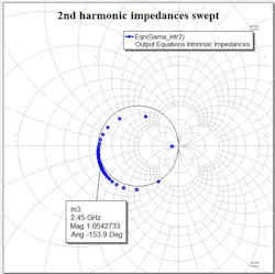
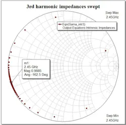
Note that the second harmonic intrinsic impedance exhibits a negative resistance in some areas. This may seem unusual, but it’s a real and known parametric effect for nonlinear capacitors.4
The effect of negative resistance at the intrinsic generator is caused by both CGD and CDS. In most models, the CDS isn’t modeled as nonlinear but rather with a constant value, and this effect isn’t strong in simulations. But, in practice, it has a strong effect that’s well-modeled with nonlinear CDS for the transistor models of Cree (now MACOM).
>>Download the PDF of this article, and check out the TechXchange for similarly themed articles and videos

If the effect of a negative resistance in the harmonic intrinsic load is much stronger, temporarily tuning the fundamental intrinsic load to exhibit a capacitive reactance as in Figure 8 dampens the effect. However, if the excursion into negative resistance is small, there’s rarely a need to use this technique.
It’s critical to observe that because of the output transistor’s capacitance, most of the 5° steps have concentrated into about a 20° region, a very dense section with about 0.25° steps. If the intrinsic harmonic impedance is in this region, the performance of the stage will be strongly insensitive to tolerances affecting the harmonic load impedances. Even a very wide tolerance will not affect the overall performance. That, in modern terms, is “anti-fragile”1.
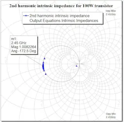
The bigger the transistor, the bigger the output CDS, and the stronger the effect. The compressed section becomes even smaller, as shown in the graph of Figure 9 where a 100-W transistor is used. Conversely, on the right of the Smith charts of Figures 6 and 7, a 5° step on the output of the transistor leads to ≈75° steps at the intrinsic generator. In Figure 9, it nearly doubles.
Step 6: Optimize harmonic impedances
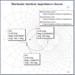
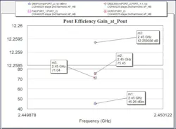
- Move the harmonic intrinsic loads from being a short circuit (Class B mode) to the middle of the dense region (Fig. 10). The more precise the move, the better. Note that the power and efficiency somewhat improve (Fig. 11).
Step 7: Tune fundamental impedance
- With the intrinsic harmonic impedances selected in the middle of the dense regions, tune the load fundamental impedance for maximum Pout.
- This greatly improves the amplifier efficiency, too (Fig. 12).
Class J Mode of Operation
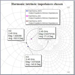
As a result of this last tuning, the Smith chart of Figure 13 makes it apparent that the corresponding intrinsic fundamental impedance becomes slightly inductive. This happens to be the classic Class-J mode of operation, discovered, researched, and explained by Steve Cripps in his book2 and other articles. Steve Cripps has been teaching us how to properly understand and design RF power amplifiers since the early 1980s.
This procedure defines the optimal Class J mode at a single frequency for optimal power and efficiency, but with the addition of tolerance insensitivity. It’s an invariable selection of the fundamental and second-harmonic intrinsic impedances with the addition of the third-harmonic impedance, all of which achieves most optimum robust performance.
In theory, the same result could be achieved for power and efficiency if the intrinsic second-and third-harmonic reactances are inductive and the fundamental intrinsic impedance is with capacitive reactance. This is moving into the sensitive regions, though, so it’s wise to leave these combinations to the PhD candidates and their professors.
Of course, when the transistor is smaller and delivers less power, the CDS is smaller, and therefore the intrinsic dense region is less dense, and the highly sensitive regions aren’t so strongly pronounced. At lower frequencies, where parasitics play less of a role, this observation becomes more evident. It’s unsurprising that most scientific articles for achieving real continuous classes of operation in wide bandwidths are presented using Cree’s (now MACOM) famous 10-W gallium-nitride (GaN) HEMT.
On the other hand, larger GaN transistors with larger drain capacitance or LDMOS transistors with significantly higher capacitance will exhibit a much higher density and operate much closer to the short-circuit region for the harmonic impedances. The operation naturally is near Class B or modest Class J. In the author’s opinion, achieving pure Class F or inverted Class F operation is a fantasy (except at very low frequencies).
Additional insights into defining transistor harmonic load impedances would be gained, with the optimum inductive intrinsic fundamental load already defined for Class J, when a simulation is performed simultaneously sweeping the angles of the second- and third-harmonic load reflection coefficients through 360° with 5° steps (Fig. 14). This simulation allows for plotting of Pout and efficiency (drain efficiency in this case) on 3D graphs.
In the graphs of Figures 15 and 16, the results of Pout and drain efficiency are displayed in blue, and reference plains of desired achievement in pink. Note the sizable area of good performance for wide changes of second- and third-harmonics reactances (angles) of the load.
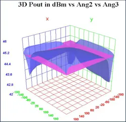
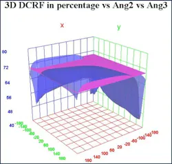
These wide changes at the transistor’s output terminal define nearly the same condensed areas at the intrinsic generator shown on the Smith charts of Figures 6 and 7, when the dips in performance are in the stretched areas, which are to be avoided.
Looking carefully, one may note that there’s a narrow area in which the combinations of fundamental and harmonics load impedance provide best performance for power or efficiency. But at least the second-harmonic load is again in the sensitive areas. Adjacent to this area are the dips in performance. Therefore, it would also be prudent to avoid this “best” performance area.
What if the Transistor Model is a “Black Box?”
Now, we’ll consider a procedure to be used when the transistor model is a “black box.” This procedure follows naturally from the above discussion:
- Use a single-tone harmonic balance simulation and tune for maximum power. The laws of nature dictate that this setup will achieve Class B intrinsic impedance as shown in Figure 2, although it’s not possible to visualize this condition.
- Switch back to a three-tone simulation and simulate for the 3D graphs shown in Figures 15 and 16.
- Choose the second- and third-harmonic reactance values in the middle of the wide areas above the reference planes for required performance. This may not be as accurate as selecting with the graphs of Figures 6 and 7, where the 5° steps of the angle of the harmonic intrinsic impedances are found in condensed areas of the Smith charts. However, it’s much better than not defining the second- and third-harmonic impedances before attempting to achieve simulated load-pull contours or to design the output matching network.
- Now, once again, tune the fundamental load impedance for maximum power or for maximum efficiency. It will be Class J mode with an inductive fundamental intrinsic load.
Recommendations for Designing an Output Matching Network
When the fundamental and harmonic load impedances are predefined over a specified frequency band, load-pull contour simulations could be properly performed as is described in Reference 3 and shown in that article’s Figure 7, which are likely to have been conducted using ADS. The extensive load-pull facility in Microwave Office provides the capabilities to easily achieve such simulations.
A versatile network synthesis tool should allow one to synthesize a network for the target impedance regions needed for the fundamental and harmonic loads. It’s also possible to directly use the defined fundamental and harmonic loads without going for load-pull simulations, but with somewhat limited control for desired performance.
When synthesizing the output network, as required bandwidths grow wider, correspondingly lower weights should be used for the second- and third-harmonic loads. Also, wider areas of the harmonics reactances should be used, but only in the congested non-sensitive areas as discussed here. The third-harmonic load has much less influence on the performance, so its weight factor should be lower than for the second-harmonic load.
For purposes of synthesis and optimizations, the third-harmonic load could even be omitted, especially if it’s suspected that the parasitic elements of the transistor model at the third-harmonic frequency aren’t accurate. Typically, the package parasitic elements are represented with only a few lumped elements, but at much higher frequences this distorts the reality.
Regardless, it’s good practice to determine where the intrinsic loads are after the synthesized output network has been added to the complete design and during optimizations.
In conclusion, these procedures provide a simple practical method to define optimal fundamental and second- and third-harmonic load impedances for RF power amplifiers, ensuring high power, efficiency, and anti-fragile performance against tolerances. By targeting condensed impedance regions, the output matching network avoids steep frequency slopes, thus enhancing robustness.
Acknowledgement
The author thanks Malcolm Edwards for improving the article’s flow by applying his excellent English and extensive Microwave Office technical knowledge.
References
1. Nassim Taleb, Antifragile: Things That Gain from Disorder, Random House, 2012.
2. Steve C. Cripps, RF Power Amplifiers for Wireless Communications – Second Edition, Artech House, 2006.
3. Neal Tuffy et al., “A Simplified Broadband Design Methodology for Linearized High-Efficiency Continuous Class-F Power Amplifiers,” IEEE Transactions on Microwave Theory and Techniques, vol. 60, no. 6, June 2012
4. Zulhazmi A. Mokhti et al., “The Nonlinear Drain–Source Capacitance Effect on Continuous-Mode Class-B/J Power Amplifiers,” IEEE Transactions on Microwave Theory and Techniques, vol. 67, no. 7, July 2019
>>Download the PDF of this article, and check out the TechXchange for similarly themed articles and videos
About the Author

Ivan Boshnakov
Engineer
Now retired, Ivan Boshnakov continues his deep dives into amplifier design, crafting application notes and exploring new techniques with Cadence/AWR Microwave Office.
Over a 30-year career in design and design-team management, Boshnakov cites work with low-noise to high-power (1.5 kW) RF amplifiers from 1 MHz to 40 GHz. Those amplifiers span implementation technologies from chip-and-wire and MMICs to printed-circuit boards. He has helped bring more than 210 amplifiers into production.
Boshnakov has published practical articles in various industry publications, often teaming up with co-authors from AWR (now Cadence), Modelithics, and Ampsa.
