PCB Technology in Software-Defined Radio
This article appeared in Electronic Design and has been published here with permission.
Members can download this article in PDF format.
What you’ll learn:
- What is software defined radio (SDR) and how does it benefit modern communications and RF applications?
- RF/microwave PCB design for SDRs.
- Challenges of SDR PCB design and ways to overcome them.
Software-defined radio (SDR) requires complex circuitry on printed circuit boards (PCBs) that defines the functionality of the device as well as the performance of these microwave and RF systems. This article discusses the factors that arise when designing PCBs for SDRs that need to maintain signal integrity.
What is an SDR?
An SDR includes what’s commonly termed a radio front-end (RFE) and digital backend. The RFE boards contain the functionality of the radio over a very wide tuning range and incorporate various analog components such as LNAs, mixers, filters, frequency synthesizers, gain/attenuation blocks, and other devices needed for receiving (Rx) and transmitting (Tx) functionality.
The highest-performance SDRs contain 3 GHz of instantaneous bandwidth using multiple independent RFE channels and digital-to-analog and analog-to-digital converters (DACs and ADCs).
The digital backend usually leads to/from the DAC/ADC to a field-programmable gate array (FPGA) that performs various digital-signal-processing (DSP) tasks. This includes modulation, demodulation, digital upconverting (DUC)/digital downconverting (DDC) using a CORDIC mixer, and various digital filtering techniques to optimize for spurs and harmonics. In addition, the FPGA packetizes IQ sample data into our Ethernet protocol stack to transfer data to and from the SDR and host system.
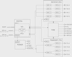
Other boards are required to ensure tight timing and control, as well as power distribution. The basic layout of the five boards used in Per Vices’s Crimson TNG SDR is shown in Figure 1.
Benefits and Uses of SDRs
Numerous benefits emerge when using SDRs versus traditional analog radios since the physical-layer functions are controlled by software. Particularly, the flexibility of SDRs is very appealing as it means that SDRs can be reconfigured by simply updating software.
For example, you can use the same SDR for different radio modulation/demodulation schemes on different center frequencies. Moreover, due to the vast amount of FPGA resources available in the digital backend, a lot of the complexity of systems, such as radar, can be integrated into the SDR’s design, thereby reducing the number of individual pieces of hardware/software required.
SDRs come in multiple form factors and are ubiquitous in any sort of wireless communications or RF communications, and thus used in many industries. Commercially available SDRs can range in complexity and size, from a USB dongle up to a server rack-sized system. SDRs are integrated into systems including low-latency links, radar, MRI, GPS/GNSS, and other satellite connectivity, spectrum monitoring and recording, electronic warfare, and various other defense applications.
RF/Microwave PCB Design Basics
RF and microwave (MW) layouts encompass the design of PCBs in the range of hundreds of megahertz up to many gigahertz, in both the analog and digital domains. The PCB is built, and components connected together, using waveguides (i.e., transmission lines) designed to pass signals within a band of interest and filter energy outside that range with minimal signal loss.
Transmission lines are specialized cables or other conductors that carry electromagnetic waves (EM waves) in a contained manner. While transmission lines can technically be anything from a high-voltage/low-frequency power line to a coaxial feedline for an antenna, in PCB design, they tend to be very small conductors broadly called traces, such as microstrips, coplanar waveguides, and stripline traces. These RF/MW transmission lines operate at a much higher frequency and don’t behave like that found in low-frequency circuits in terms of how they travel along the traces.
An important property of a transmission line or trace in PCBs is known as the characteristic impedance, often denoted Z0. Impedance, an alternating-current (AC) characteristic, affects how RF/MW signals propagate through the board, how power is transferred between components, and how signals bleed or cause crosstalk into unwanted areas of your PCB. Crosstalk/bleed is discussed later.
Different types of waveguides/transmission lines, including microstrip, coplanar waveguides, and stripline traces, have different characteristics due to their physical properties and thus their characteristic impedance (Fig. 2).

PCB connector technologies for electrical components tend to be through-hole, edge-mount, or surface-mount technology. Different chips (amplifiers, mixers, filters, switches, etc.) or components use different types of connections, so tradeoffs must be considered.
For instance, through-hole technology benefits from not requiring a stencil, and it’s relatively easy to perform rework if necessary. However, it suffers from lower temperature operation, larger footprint, and the fact that it requires manual assembly. On the other hand, surface-mount technology benefits from automated assembly/soldering, higher temperature operation, and greater component density/smaller footprint, but is at a disadvantage as rework is more difficult and warps/twists of the PCB aren’t as easily tolerated.
Typically, 50-Ω SMA connectors are where signals terminate on the RFE board. These SMAs can be edge mount, through-hole, or surface mount. It’s often the case that the target frequency range determines the mounting option.
In the case of RF design, multilayer PCBs are the best option since these systems are complex, contain a number of components (both active and passive), and are required to have a number of capabilities.
For multilayer PCBs, general layers are made from FR4 laminates and include ground planes (GND planes—technically a power plane but also known as a reference plane), power planes (PWR planes), and inner signal layers. The actual layer stackup will be determined by PCB material and many other elements: routing, components (digital vs. analog signals and components), mounting technologies, etc.
Challenges with SDR PCB Design
Layer count and thickness
It’s important to balance layer counts in such ways that ensure proper signal integrity, ground, and thermal constraints.
For example, in the design of Per Vices SDR PCBs, one of the biggest drivers for large layer stackup is high-pin-count ball grid arrays (BGAs), where special consideration must be given to the “breakout” or “fanout” of the traces from the pads to achieve the densest breakout possible. However, the density of the breakout also is determined by the clearance needed and what kind of signal you’re breaking out.
Of course, layer counts also cause problems with manufacturability and increase cost. Thus, using only the required amount of layers is preferable. Moreover, with more layers comes the challenge of ensuring that signals are properly interconnected between layers.
Signal integrity
Energy coupling between different traces can cause crosstalk (Fig. 3) and noise induction, leading to signal degradation. The coupling occurs due to mutual capacitance and mutual inductance between the traces.
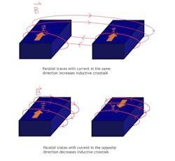
In terms of mutual inductance, the inductive coupling or magnetic coupling between conductors happens due to the magnetic field produced by the current flowing in conductors—a phenomenon related to Biot-Savart and Ampere’s laws. Essentially, when there’s another trace nearby, the magnetic field produced by this conductor passes through the other conductor and induces a current, creating inductive coupling between the PCB traces.
Signal degradation also may occur due to attenuation losses caused by conducting trace resistances, which increase at higher frequencies because of skin effect (i.e., the resistivity equation says that a reduction of the effective cross-section of a conductor increases resistance) and dielectric material dissipation.
Many other events also cause signal degradation, such as EMI/EMC. For example, there’s signal degradation due to via stub traces: Long stub traces may act as antennas and consequently escalate problems to comply with EMC standards. Stub traces also can create reflections that negatively affect signal integrity (i.e., parasitic capacitance and inductance). Furthermore, propagation delays and uncontrolled line impedances, which are discussed in more detail below, must be overcome.
Impedance matching and signal degradation
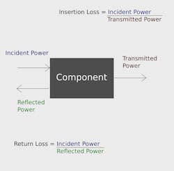
All RF circuits take advantage of EM wave propagation. This means input impedances must be used when determining how to match impedances around a circuit and how to create interfaces between different sections of an RF circuit. Essentially, this requires that we ensure the incident power is matched to the component to minimize insertion and return loss (Fig. 4).
A continuous RF/MW signal transferred through a transmission line to a component’s mismatched load impedance will result in a substantial reflected signal. This causes the incident and reflected EM waves to pass each other in opposite directions and the interference culminates in a standing wave. This is a stationary wave pattern equal to the sum of the incident and reflected waves.
Such standing waves may result in voltages that are higher than the original voltage of the transmitted signal, and in some cases, the effect is severe enough to cause physical damage to a component. However, it depends on the relationship between the Z0 transmission line (trace) and Z load (component), and thus isn’t always a higher voltage.
Return loss must be minimized, since, at very high frequencies, the return signals take the path of least inductance (this return path is the reference plane noted above). As a result, they will go through power planes, through the PCB’s multiple layers, or take some other route, and impedance will no longer be controlled.
Overcoming Challenges
Many PCB design challenges can be conquered, or at least tradeoffs can be made to ensure that performance isn’t severely affected.
PCB layer and thickness
Besides the obvious choice of following your component manufacturer's recommendations, many other rules for good RF PCB design and layout are important. For starters, it’s essential to use a proper stackup such that the arrangement of copper layers and insulating layers are decided prior to board layout design.
A layer stackup allows you to get more circuitry on a single board through the various PCB layers. Other advantages of a layer stack include limiting a circuit’s vulnerability to external noise, minimizing electromagnetic radiation, and reducing impedance and crosstalk/inductance concerns on RF/MW PCB layouts.
Choosing the right PCB material, such as FR4 laminates, also helps. The correct materials can bring many benefits for electromagnetic loss/trace impedance as well as increase mechanical strength and thermal properties. Different materials also help to ensure high signal integrity in different environmental conditions, such as higher temperature and humidity regions.
Controlled trace impedance
Some tips to ensure impedance is controlled within the traces include keeping RF traces away from digital circuitry, using antenna bias tees, and utilizing better PCB materials (dielectric properties, etc.). In addition, more appropriate impedance transformation at stubs/interfaces with components helps overcome impedance mismatch seen by an RF signal as it propagates.
Another rule-of-thumb is to ensure that when transmission line traces are required to bend (change direction) due to, say, routing constraints, then it’s important to use a bend radius that is at least 3X the trace width.
Improving signal integrity
It’s crucial that mutual inductance/capacitance and other EMI effects are minimized to ensure proper electromagnetic shielding and isolation, since RF signals need to be as noise-free as possible. Many unique shielding structures and layout techniques have been formulated, which help provide the required shielding and isolation in RF systems, including via fences, solid power pours surrounding the RF signal trace, EMI shields, and others.
One way to deal with the inductive crosstalk is to ensure the ground plane or the return plane is placed as close to the conducting trace as possible. This is because the magnetic flux generated by the trace carrying a current tends to cancel with the magnetic flux in the return path trace.
In addition, to limit inductive crosstalk, it’s important to route traces that are parallel whereby the current is going in the opposite direction as well as ensure that the traces are 3X apart as their width.
The choice of trace is a key factor, too. For instance, it’s possible to decrease crosstalk by using stripline traces. On the other hand, microstrips have a lower loss tangent (from polarization and relaxation of charges in atoms, stray conductance on the substrate, and fiber weave effects) and a faster propagation time, which can help improve signal integrity. Again, there are tradeoffs between various ways of improving signal integrity.
Other tips include using device packages/components with short leads to reduce parasitic capacitance and inductance. Furthermore, ensuring traces/stubs leading to these components are equal in length and as short as possible can help with these parasitic EMI. There are also ways to minimize the via stubs by back drilling (Fig. 5) using high-density interconnect technologies (e.g., buried and blind vias), but these all add significant cost to a project.

On top of that, multiple low-inductance decoupling capacitors can be used across power and ground rails. They should be placed as close to the device power and ground pins as possible.
Isolation and separation from other circuits
Isolation is possible by keeping transmission-line traces as far apart as feasibly possible, and by not routing in close proximity for extended distances over the PCB. This entails that inductive coupling between parallel microstrip lines will increase with decreasing separation or increasing parallel routing distance.
Other separation techniques include ensuring that traces crossing on separate layers should have a ground plane keeping them apart. For instance, add a solid ground pour to the design on each signal and power layer, stitched with ground vias to connect “islands” and provide separation between signals. Moreover, traces that carry high power levels should be kept away from all other low-power traces whenever possible.
Because PCBs for SDRs also include high-speed digital signal lines, it’s important that these are routed separately on a different layer than the RF signal lines to prevent coupling. Digital noise (clocks, PLLs, etc.) can couple and modulate onto RF signal traces and then onto the carrier if one isn’t careful. It’s also important that RF traces are appropriately isolated from other high-speed signals. In Per Vices’ case, the digital board is separate from the RFE boards, which is important for isolation.
Conclusion
As discussed, many challenges arise when designing high-speed RF/MW PCBs for SDRs. We’ve touched on only a few issues concerning waveguides, impedance matching, signal integrity, as well as the means to mitigate and overcome these obstacles. Of course, many other issues emerge during these complex PCB designs, and volumes of books have been written on the topic.
About the Author
Brendon McHugh
Field Application Engineer & Technical Writer, Per Vices Corp.
Brendon McHugh is a field application engineer and technical writer at Per Vices, which has extensive experience in developing, building, and integrating software-defined radios. Brendon is responsible for assisting current and prospective clients in configuring the right SDR solutions for their unique needs. He holds a degree in theoretical and mathematical physics from the University of Toronto.
