Algorithms to Antenna: Modeling Antennas Installed in the Presence of Large Platforms
The workflow discussed here can be used to model antennas mounted in the presence of platforms or structures. This is a request that often comes up in the context of integrating a new antenna near a large platform such as a ship, aircraft, or vehicle. As we have described in past blogs, you can model the antenna accurately using a Method of Moments (MoM) electromagnetic solver. To consider the effects of an electrically large platform, a physical-optics (PO) solver helps provide you with a good result without a large increase in simulation time.
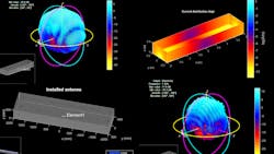
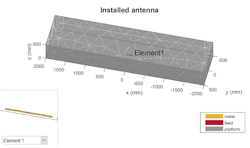
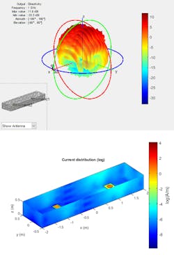
As the first step in the workflow, the electrically large platform is imported into Antenna Toolbox as an STL file. As was also described in our recent blog on radar cross section (RCS) benchmarking, STL files can be utilized to describe ships, planes, or any other kind of structure. To illustrate the example clearly, we use a large rectangular platform cavity (Fig. 1). A single antenna element dipole is located near the center of Figure 1 and is labeled as Element 1.
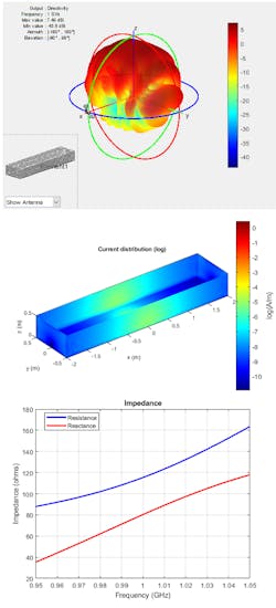
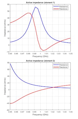
Once the structure and antenna element are defined, the same types of analysis that you would typically do with an antenna element or an antenna array can be performed here. Figure 2 shows the 3D pattern, the current analysis, and the impedance plots of the 1-GHz system. Note that the system is solved through a combination of MoM for the antenna element and PO for the structure.
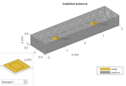
You can extend this type of installed antenna analysis with multiple antenna elements. To make it more interesting, a rectangular patch microstrip antenna and a circular patch microstrip antenna are designed at 1 GHz and placed inside the rectangular cavity structure two meters apart (Fig. 3).
Again, you can perform all of the same analyses using multiple antenna elements as shown in Figures 4 and 5.
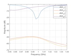
It’s also interesting to note the coupling between the antenna elements, which is calculated using the S-parameters. In Figure 6, you can see how the structure and the elements (and their interactions) impact the system’s bandwidth.
If you have STL files for other structures, the same workflow can be utilized to model and analyze how your element of interest interacts with those structures.
To learn more about the topics covered in this blog, see the examples below or email me at [email protected]:
- Installed Antenna Analysis: Modeling Antennas with Platforms (example): Learn to model an antenna element in the presence of a large platform. The antenna is modeled accurately using the Method of Moments (MoM), while the effect of the electrically large platform is considered using physical optics (PO).
- Pattern Analysis of the Symmetric Parabolic Reflector (example): Learn to model the effects of feed position and reflector surface geometry on the far-field radiation pattern of a half-wavelength, dipole-fed symmetric parabolic reflector.
- Antenna, Installation Platforms, and Radar Cross Section Analysis (webinar): Learn to develop beamforming algorithms, taking into account edge effects and the coupling between array elements. You also see how to install the antenna on a large platform such as an airplane or a car. Practical demonstrations show how to easily import the description of an arbitrary installation platform using CAD formats such as STL files and analyze its effects on the antenna performance.
See additional 5G, radar, and EW resources, including those referenced in previous blog posts.
About the Author
Rick Gentile
Product Manager, Phased Array System Toolbox and Signal Processing Toolbox
Rick Gentile is the product manager for Phased Array System Toolbox and Signal Processing Toolbox at MathWorks. Prior to joining MathWorks, Rick was a radar systems engineer at MITRE and MIT Lincoln Laboratory, where he worked on the development of several large radar systems. Rick also was a DSP applications engineer at Analog Devices, where he led embedded processor and system level architecture definitions for high performance signal processing systems used in a wide range of applications.
He received a BS in electrical and computer engineering from the University of Massachusetts, Amherst, and an MS in electrical and computer engineering from Northeastern University, where his focus areas of study included microwave engineering, communications, and signal processing.
Honglei Chen
Principal Engineer
Honglei Chen is a principal engineer at MathWorks where he leads the development of phased-array system simulation. He received his Bachelor of Science from Beijing Institute of Technology and his MS and PhD, both in electrical engineering, from the University of Massachusetts Dartmouth.
Giorgia Zucchelli
Product Marketing Manager, RF & Mixed Signal
Dr. Giorgia Zucchelli is the product marketing manager for RF and mixed-signal at MathWorks. Over the last four years, Giorgia has guided several users with the adoption of MathWorks tools for modeling and simulating RF and AMS systems, including antennas, adaptive front ends, and analog electronics. Giorgia holds a master’s degree in electronic engineering and a doctorate in electronic engineering for telecommunications from the University of Bologna.
Vishwanath Iyer
www.mathworks.com
Vishwanath Iyer is the principal software engineer at MathWorks. He has expertise in use of MATLAB and Simulink for model-based design and analysis as well as hands-on experience with RF lab hardware such as vector network analyzers, vector signal generators, spectrum analyzers, and oscilloscopes. In addition, he is a strong RF antenna and array designer with practical experience in the use of full-wave electromagnetic simulators. Vishwanath received his Ph.D in antennas and RF circuit design from Worcester Polytechnic Institute.
