Refine Biasing Networks for High PA Low-Frequency Stability (.PDF Download)
High-frequency active-device performance depends very much on the dc biasing conditions. For optimum performance, a solid-state device (SSD) requires an application-specific biasing network. Such bias networks are not only essential parts of RF/microwave circuits with SSDs, but properly designed bias networks contribute a great deal to the performance and stability of high-frequency circuits using SSDs.
SSD gain is inversely proportional to frequency, with higher gain at lower frequencies, so attention should be paid to SSD circuit design because of the strong connection between device gain and stability. For example, the response of an RF/microwave power amplifier (PA) should be carefully compensated to prevent oscillations due to the higher gain at lower frequencies.
At lower frequencies, the impact of the biasing networks is dominant compared to the impedance-matching networks. That’s because the small value of the dc blocking capacitor has a high impedance at lower frequencies, and neutralizes the effects of the matching networks. Thus, a properly designed biasing network can be employed to improve SSD low-frequency stability.
Although the stability analysis of RF/microwave circuits is a major topic, partial analysis allows for inferring some ideas about the low-frequency stability issues induced by biasing networks. The influences of PA biasing networks on low-frequency stability can be shown by analyzing the simplified low-frequency equivalent of a high-power field-effect transistor (FET) and its biasing networks.
Class AB type biasing will be considered for the low-frequency stability analysis. Following the analysis, design suggestions will be presented regarding gate and drain biasing, with attention paid to RF/microwave performance parameters such as insertion loss and efficiency. Finally, a resonance investigation study of a PA and its measured results will be presented.
Power-Amp ABCs
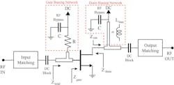
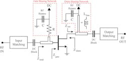
A typical PA consists of an active device and at least four passive subcircuits: input impedance matching, gate biasing, output impedance matching, and drain biasing. Figure 1 depicts such a structure. It is assumed that the values of the dc blocking capacitors are small enough to ignore the influence of matching networks on the analysis of the low-frequency response of the PA.
1. This is a conventional biasing structure for an RF/microwave power amplifier (PA).

