A 60-GHz Power Amplifier for Aerospace and Telecom Apps

This article is part of the TechXchange: RF Amplifier Design
Members can download this article in PDF format.
What you’ll learn:
- A strategy for development of a multi-way power amplifier.
- What to pay attention to and what parameters to measure when developing a PA with this technology.
In recent years, we’ve seen the demonstration of several 60-GHz CMOS building blocks and integrated receivers13-15 as well as publishing of complete 60-GHz integrated receivers.6,16,17 The amplifier described here comprises a CMOS transistor, transmission lines, ac-coupling and supply-ground bypass capacitors, resistors, RF ground-signal-ground pads, and dc pads.
This work explores the challenges facing the design and implementation of a 60-GHz power amplifier (PA) in standard 90-nm CMOS processes. We’ll present a low-loss power combining technique, which takes advantage of millimeter-wave (mmWave) amplifier topologies, to implement four power amplifiers in a standard 90-nm, 1-V CMOS process. The resulting design offers record performance in terms of 1-dB compression and saturation output power.
Design, Layout, and Modeling of the Components
Optimizing the Widths and Number of Fingers
The gate resistance for multi-finger CMOS behaves as a distributed RC network, therefore this approximated form is suggested:3-7

where Rpoly is the polysilicon gate sheet resistance, WF is the finger width, L is the channel length, and n = 1,2, depending on the number of gate contacts. Furthermore, we provide Equation 2 for frequency fT, which has no effect on the gate resistance:4

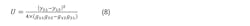
In Equation 2, gm is the transistor transconductance and Cgs is gate-to-source capacitance. The power losses introduced causes a reduction in the transistor fmax and maximum stable gain (MSG). Therefore, if we neglected the drain resistance and the losses in the substrate, we can write:8,18,19

Cgd and Cgs are the gate-to-drain and gate-to-source capacitances, respectively; Rg, Rs, rch, and gds are gate-source channel resistance and transistor output conductance. Thus, maximizing fmax places an upper limit on the maximum finger width of a transistor and, in turn, on its output power capability. Once the finger width is optimized to maximize fmax, the number of fingers should be maximized to increase the effective transistor size.
However, when operating at mmWave frequencies, as the number of fingers increases, the height of the transistor layout grows proportionately and results in a large layout aspect ratio. Because the number of fingers remains less than ≈100, the size of the gate, drain, and source networks used to connect these gates to all fingers can be kept relatively small, resulting in low gate, drain, and source resistances. But as more fingers are added, larger networks with high tapers are needed. These introduce additional resistive gate and drain losses, as well as degeneration of the resistive source, leading to lower fmax and MSG.
Because the length of the transistor is much greater than the width of the transmission line feeding its gate and drain, we need large gate and drain networks to reduce the gate and drain inductances.
Tradeoff Between Power Gain and Output Power
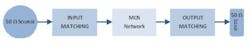
A transistor is typically driven with a 50-Ω source and drives a 50-Ω load. However, input and output matching networks are typically used to transform these load impedances of the source and drive output (Fig. 1). They also provide the power supply with source and load impedances that ensure stability and maximize power gain and output power.
The conditions on these impedances that lead to maximum power gain are different from those that lead to maximum output power, hence the trade-off between power gain and output power.
The power gain can be defined as:1
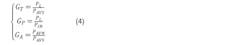
where GT, GP, and GA, are respectively the power gain, operative power gain, and available power gain, while the stability factor K is:

with:

If we assume that the device is unconditionally stable, the source and load impedance should be conjugately matched, therefore:

The MSG is defined as the value of GT, max when K = 1. Although the value of GP can approach infinity when the transistor is operated in the potentially unstable case, values of GP that are above the figure-of-merit MSG, result in values of ГL and ГS, which are very close to the unstable region and therefore decrease the robustness of the project.
In Reference 1, it’s shown that the ГL values producing constant power gain lie on a circle, called the operating power-gain circle, when plotted on a Smith graph. The resulting Zin can be calculated. To obtain the maximum power gain under the chosen ГL data, the input-matching network can then be designed to conjugate Zin and ZS if this results in a ГS in the stable region.
Pad Modeling
At 60 GHz, the pads are treated as part of the design, which is to say that the losses of the pads aren’t independent from the measurement results of the amplifiers. Because they’re treated as parts of the input and output matching network, it’s important that they be accurately modeled.
To reduce pad parasitics and thus pad losses, the pad-side signal is reduced to just 55 μm, the minimum size required for probing. We used the circuit shown in Figure 2 to model the RF ground-signal-ground pad.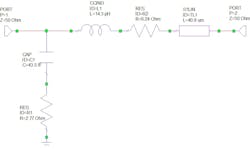
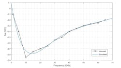
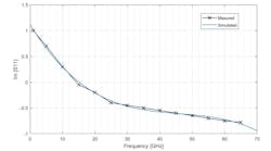
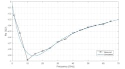
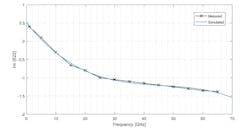
Figures 3 and 4 show the measured versus simulated Z parameters, in particular Im{Zin} that’s relevant for this analysis.

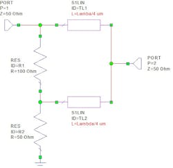
Wilkinson Power Combiner
Because the capability of the measurement equipment is limited to two-port measurements, the Wilkinson power combiner (Fig. 5) is treated as a two-port network with the third port terminated by an on-chip 50-Ω resistor. We used Cadence Design Systems’ AWR Microwave Office to design the transmission lines with a characteristic impedance of 70.7 Ω; MathWorks’ MATLAB elaborated the data. The 50-Ω and 100-Ω resistors use polysilicon.
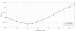
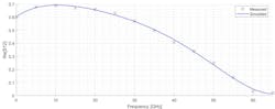
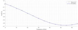
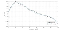
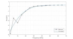
Figures 6 through 9 show the measured S-parameters compared with simulated values over the entire frequency range. Note the reporting Transistor Unit of both the real and imaginary parts of the parameters S11 and S12.

The transistor’s fT and fmax values are the two most common and important metrics used to measure the device’s speed characteristics. They can be related to the intrinsic and extrinsic parameters of the transistor via Equations 2 and 3.
From Equation 2, it’s shown that the fT transistor depends only on its intrinsic parameters. Circuit designers have no control over these parameters and must work with the transistors at hand. On the other hand, Equation 3 shows that the transistor fmax depends on fT as well as the extrinsic resistive networks at the gate and source of the transistor. These resistances depend on the arrangements of the transistor’s gate and source networks.
An accurate layout can have a major effect on the value of fmax. For example, the change in fmax from 80 GHz to 280 GHz has been reported due to layout differences in the same 90-nm CMOS process.20,21 Because we use transistors in amplifiers to provide power gain instead of current gain, a lot of time is spent on improving the transistor fmax.
In our case, the gate and drain networks are composed of 5-μm-wide vertical multilayer metal plates with wide channels to minimize the resistances and extrinsic inductances of the gate and drain. A network of sources located in the lower metal layer collects all of the finger sources and connects them to the two upper and lower ground planes. The gate and drain of the transistor connect to the circuit through 10-μm-wide coplanar transmission lines. These transmission lines aren’t considered part of the transistor model.
We extrapolated Mason's one-sided gain to extract the fmax value. Mason's one-sided gain can be written in terms of the Y-parameters of the two-port device as:9
where gij = Re{yij}. Because in this case fmax is, as often happens, beyond the frequency capability of the measuring equipment, it’s derived from the extrapolation of the unilateral Mason gain assuming a slope of 20 dB/decade. The suboptimal layout suffers from bulky gates and drain cones, as well as narrow 2-μm-wide gate and drain networks with a small number of vias and pole contacts.
Unsurprisingly, this layout measured an fmax of just 143 GHz. However, because the device is conditionally stable at 60 GHz, reducing its gate and drain resistance doesn’t alter its 60-GHz MSG by 7.6 dB. These parasitics are insignificant at low frequencies and can be ignored without too much performance penalty.
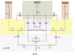
Nonetheless, they significantly change and can potentially dominate the behavior of the transistor at mmWave frequencies. Therefore, these connections should be considered part of the transistor and modeled. The preferred active-device modeling approach at mmWave frequencies requires measuring the S-parameters of the small signal of a given transistor at a given bias point, then optimizing the parameter values of the custom-designed model shown in Figure 10 to fit the measured and simulated S-parameters.10
Figures 11 through 18 show the comparison between measured and simulated S-parameters split into real and imaginary parts. They are: Re{S11}, Im{S11}, R{S12}, Im{S12}, Re{S21}, Im{S21}, Re{S22}, and Im{S22}. From these, we notice that this model provides a very accurate result as exemplified by the good fit between the measured and simulated data.


Four-Way Power-Amplifier Design
Circuit Description
Figure 19 shows the block scheme of the four-way power amplifier. It consists of four identical unit amplifiers along with the division and combination of power.
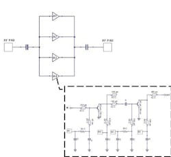
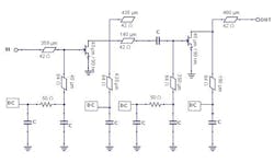
Figure 20 shows the circuital scheme of the single-way power amplifier. The input matching network is designed in such a way that a long series transmission line is presented at the input of the unit's amplifier.
The 358-μm-long transmission lines to the inputs of the four-unit amplifiers are routed to feed a common dividing node, and the 460-μm-long transmission lines to the outputs of those amplifiers are routed to feed a common combiner node to accomplish the division of the power and combination functions, respectively. In this way, no external power splitter or combiner is added to the power amplifier and, therefore, no additional power loss is introduced.
Each unit amplifier consists of two conditionally stable common-source stages. The first and second stages use 40- and 80-μm (1-μm/finger) transistors, respectively. The matching networks were created using coplanar transmission lines. Series transmission lines use only the top metal and have a 2-μm gap between the signal line and ground planes with a characteristic impedance Zo of 42 Ω.
Short-terminated inductive lines are made with coplanar transmission lines that reside in the upper metal layer but employ more than 9 μm of space between the signal line and ground planes. Thus, they have a Zo greater than about 69 Ω and a greater inductive quality factor. We used large MOS capacitors for low-frequency bypass to ensure low-frequency stability. The dc voltages are supplied to the gates and drains of all transistors through the transmission lines of the matching networks.
For the gate-bias network, we use a 50-Ω series resistor to suppress potential instability at low frequencies. To achieve high output power, the output matching networks, together with the power combining node, are designed to convert the 50-Ω load at the power amplifier output into the optimum power impedances seen at the transistor drain from 100 μm of the second stage. Note that the gain of the output transistor would decrease significantly if it were to drive a 50-Ω load.
When selecting the optimum load impedance, we make a tradeoff between gain and output power. In addition, we’ve introduced a matching network between the driving stage and the output stage to ensure maximum power transfer between stages and the stability of each stage. The input match networks, together with the power split node, provide a 50-Ω input match. Although all transistors are conditionally stable, we chose the impedances seen by each amplifier to ensure stable operation.
Measurement and Simulation Result
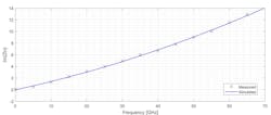
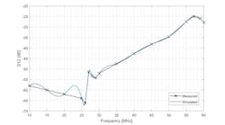
Measurement and simulation results for the S-parameter are shown in Figures 21 through 24. First, Figure 22 shows that the measured S11 peak is −7 dB at 64 GHz. Meanwhile, Figure 23 shows that S12 is better than −25 dB on the full range of frequencies. This is due to the input being matched to an impedance of 50 Ω.
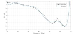

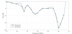
Secondly, Figure 24 reveals a measured S21 peak of 4.4 dB at 58 GHz. Although peak gain behavior is observed around 27 GHz, PA stability is preserved as S21, S11, and S22 remain below 0 dB. Furthermore, the stability factor, K, remains higher than 4 over the entire frequency range.
Figures 25 through 28 show the global input-output power amplifier parameter. Figure 25 displays compression and saturation output powers of 1 dB of +13.1 dBm and +15.2 dBm, respectively. In Figure 26, we report the comparison between simulated and measured power gain. The difference is about 0.8 dB below to favor simulated data. This is due to the constructive imperfections inherent in the process used for the realization of the PA.

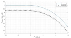

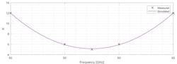
Figure 27 denotes that the additional efficiency of the peak measured power is 6.2%, which is due in part to the low gain. The amplifier consumes 145 mW from a 1-V supply and the linear behavior between the input and output power levels indicates the stability of the amplifier. In fact, Figure 28 shows the trend of the stability factor K, which always remains above 4 points.
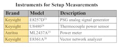
Measurement Setup
The table shows the instruments used to perform all measurements of this work.
Conclusion
The prototype four-way power amplifier is implemented in a standard 90-nm, 1-V CMOS process. We integrate power dividers and combiners into input and output matching networks rather than using this device separately. The unit's amplifiers employ optimally sized transistors of 100 fingers, 1 μm per finger, in the last stage.
The four-way amplifier combining output power provides good performance in terms of 1-dB compression and saturation output power. The first of the three two-way power amplifiers exhibits high gain with high output power, while the second provides lower gain but a higher margin of stability. Finally, the fourth power amplifier uses inductive degeneration of the source for linearization.
Read more articles in the TechXchange: RF Amplifier Design
References
1. Guillermo Gonzalez, “Microwave Transistor Amplifiers Analysis and Design,” Prentice Hall, 1997.
2. Steve Cripps, “RF Power Amplifiers for Wireless Communications,” Artech House, 1999.
3, Jan M. Rabaey, Anantha Chandrakasan, and Borivoje Nikolic, “Digital Integrated Circuits, A Design Perspective, second edition,” Prentice Hall, 2003.
4. P. R. Gray, P. J. Hurst, S. H. Lewis, and R. G. Meyer, “Analysis and Design of Analog Integrated Circuits, 4th Edition,” Wiley, Feb. 2001.
5. C. H. Doan, S. Emami, A. M. Niknejad, and R. W. Brodersen, “Millimeter-wave CMOS design,” IEEE J. Solid State Circuits, Jan. 2005, Vol. 40, pp. 144-155.
6. B. Razavi, “A 60-GHz CMOS receiver front-end,” IEEE J. Solid State Circuits, Jan. 2006, Vol. 41, pp. 17-22.
7. C. Enz, F. Krummenacher, and E. A. Vittoz, “An MOS transistor model for RF IC design valid in all regions of operation,” IEEE Trans. Microwave Theory Tech.,Jan. 2002, Vol. 50, pp. 342-359.
8. C. H. Doan, S. Emami, A. M. Niknejad, and R. W. Brodersen, “Design of CMOS for 60 GHz applications,” IEEE Int. Solid State Circuits Conf. Dig. Tech. Papers, Feb. 2004.
9. S. J. Mason, “Power gain in feedback amplifiers,” IEEE Trans. Circuit Theory, June 1954, Vols. CT-1, pp. 20-25.
10. B. Heydari, M. Bohsali, E. Adabi, and A. M. Niknejad, “Millimeter-Wave Devices and Circuit Blocks up to 104 GHz in 90 nm CMOS,” IEEE J. Solid State Circuits, Dec. 2007, Vol. 42, pp. 2893-2903.
11. C. M. Lo, C. S. Lin, and H. Wang, “A Miniature V-band 3-Stage cascode LNA in 0.13um CMOS,” ISSCC Digest of Tech. Papers, Feb. 2006. pp. 322-323.
12. S. Emami, C. H. Doan, A. M. Niknejad, and R. W. Brodersen, “A highly integrated 60GHz CMOS front-end receiver,” ISSCC Digest of Tech. Papers, 2007. pp. 190-191.
13. B. Razavi, “A mm-Wave CMOS Heterodyne Receiver with On-Chip LO and Divider,” ISSCC Digest of Tech. Papers, 2007. pp. 188-189.
14. S. P. Voinigescu, S. W. Tarasewicz, T. MacElwee, and J. Ilowski, “An assessment of the state-of-the-art 0.5um bulk CMOS technology for RF applications,” IEDM Tech. dig., Dec. 1995. pp. 721-724.
15. J. N. Burghartz et al., “RF potential of a 0.18-um CMOS logic technology,” IEDM Tech. Dig., Dec. 1999. pp. 853-856.
16. J. C. Guo, W. Y. Lien, M. C. Hung, C. C. Liu, C. W. Chen, C. M. Wu, Y. C. Sun, and Ping Yang, “Low-K/Cu CMOS logic based SoC technology for 10Gb transceiver with 115GHz fT, 80GHz fmax RF MCOS, High-Q MIM capacitor and spiral Cu inductor,” VLSI Digest of Technical Papers, June 2003. pp. 39-40.
17. L. F. Tiemeijer et al., “Record RF performance of standard 90 nm CMOS technology,” IEDM Technical Digest, Dec. 2004. pp. 441-444.
18. Y. Jin, M. A. T. Sanduleanu, E. A. Rivero, and J. R. Long, “A Millimeter-Wave Power Amplifier with 25dB Power Gain and +8dBm Saturated Output Power,” Proceedings of ESSRICC, Sept. 2007. pp. 276-279.
19. B. A. Floyd et al., “SiGe bipolar transceiver circuits operating at 60 GHz,” IEEE J. Solid State Circuits, Jan. 2005, Vol. 40, pp. 156-167.
20. U. R. Pfeiffer, S. K. Reynolds, and B. A. Floyd, “A 77 GHz SiGe power amplifier for potential applications in automotive radar systems,” Radio Frequency Integrated Circuits Symp. Dig., 2004. pp. 91-94.
21. M. Tanomura, Y. Hamada, S. Kishimoto, M. Ito, N. Orihashi, K. Maruhashi, and H. Shimawaki, “TX and RX Front-Ends for 60GHz Band in 90nm Standard Bulk CMOS,” ISSCC Dig. of Tech. Papers, Feb. 2008. pp. 558-559.
22. T. Suzuki, Y. Kawano, M. Sato, T. Hirose, and Joshin, “60 and 77GHz Power Amplifiers in Standard 90nm CMOS,” ISSCC Dig. of Tech. Papers, 2008. pp. 562-563.
23. https://www.keysight.com/us/en/assets/9018-04962/user-manuals/9018-04962.pdf
24. https://www.keysight.com/it/en/assets/9018-03854/service-manuals/9018-03854.pdf
25. https://www.anritsu.com/en-GB/test-surement/support/downloads?model=ML2437A
26. https://www.keysight.com/it/en/support/E8361A/pna-series.html
About the Author
Pasquale Dottorato
Lead RF & Microwave Engineer, RF Consultant
Pasquale Dottorato is a lead RF and microwave engineer and has participated in development of antennas and device for aerospace, defense, and mobile applications.
