Skyworks Launches Next-Gen Timing Devices for High-Speed Infrastructure
The Overview: Upgraded Timing Devices for Next-Gen Infrastructure
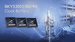
With the debut of its SKY53510/80/40 family of clock fanout buffers for next-generation, high-speed infrastructure, Skyworks Solutions hopes to simplify the design and enhance the signal integrity of timing systems across a wide range of platforms.
Who Needs It & Why? Meeting Demands for Improved Signal Integrity
Technology marches on, and now that the seventh generation of PCIe is out along with increasing demands for artificial-intelligence platforms, 5G/6G networks, and cloud computing, the precision of system timing becomes a key enabler (or critical weakness) of overall performance. System architects and hardware designers are looking to get to market faster, cut down on design overhead, and futureproof their designs in service of emerging standards such as PCIe Gen 7 and 6G.
Applications for the buffer family include:
- PCIe Gen 3 through Gen 7
- 56G/112G/224G SerDes
- 5G/6G mMIMO radio systems
- SyncE and broadcast video
- Medical imaging and aerospace/defense
Under the Hood: Scalability and Low Jitter
The scalable, low-jitter SKY53510/80/40 family features a 3:1 input multiplexer (including crystal input), one single-ended output, and up to 10 differential outputs. They come in compact thermally enhanced QFN packages — 7 × 7 mm (10 outputs), 6 × 6 mm (8 outputs), and 5 × 5 mm (4 outputs) — and are pin-compatible with industry-standard layouts for easy integration and multi-sourcing.
These devices support input clock slew rates down to 0.75 V/ns and output levels of 1.8, 2.5, and 3.3 V. As a result, they enable robust PCB designs with minimal signal-integrity challenges such as reflection, crosstalk, and ground bounce.
Among the SKY53510/80/40 family’s features is ultra-low additive RMS phase jitter: 35 fs at 156.25 MHz and 3 fs at 100 MHz (PCIe Gen 7). The devices offer universal format translation amongst a wide range of logic families and provide low-power operation with separate core/output voltage supplies (1.8, 2.5, or 3.3 V).
Further, the devices are suited for pairing with Skyworks’ Si551x network synchronizers, its SKY63104/5/6 family of jitter-attenuating clocks, and its SKY62101 ultra-low-jitter clock generators. These components can be combined to form complete clock-tree solutions that meet the demanding requirements of next-generation 6G wireless infrastructure, 800G/1600G networking infrastructure, and AI data-center applications that utilize 112G/224 PAM4 SerDes technology.
Samples and production quantities of the SKY53510/80/40 clock buffers are available now. Evaluation is supported via the SKY53510-EVB development kit.
Learn more about system clocking


About the Author

David Maliniak
Executive Editor, Microwaves & RF
I am Executive Editor of Microwaves & RF, an all-digital publication that broadly covers all aspects of wireless communications. More particularly, we're keeping a close eye on technologies in the consumer-oriented 5G, 6G, IoT, M2M, and V2X markets, in which much of the wireless market's growth will occur in this decade and beyond. I work with a great team of editors to provide engineers, developers, and technical managers with interesting and useful articles and videos on a regular basis. Check out our free newsletters to see the latest content.
You can send press releases for new products for possible coverage on the website. I am also interested in receiving contributed articles for publishing on our website. Use our contributor's packet, in which you'll find an article template and lots more useful information on how to properly prepare content for us, and send to me along with a signed release form.
About me:
In his long career in the B2B electronics-industry media, David Maliniak has held editorial roles as both generalist and specialist. As Components Editor and, later, as Editor in Chief of EE Product News, David gained breadth of experience in covering the industry at large. In serving as EDA/Test and Measurement Technology Editor at Electronic Design, he developed deep insight into those complex areas of technology. Most recently, David worked in technical marketing communications at Teledyne LeCroy, leaving to rejoin the EOEM B2B publishing world in January 2020. David earned a B.A. in journalism at New York University.
