Performance Scaling — with Balance — in Edge AI
What you'll learn:
- The importance of AI at the edge.
- What are the capabilities of embedded neural processing?
- The performance enhancement potential with in-memory compute.

As microcontrollers leverage embedded neural processing units (NPUs) to accelerate AI inference at the edge, data-movement overheads present a barrier to further progress. In-memory compute is an effective accelerator that demands close engagement with the underlying technology.
Accelerating AI at the Edge
Edge AI has reached the plateau of productivity in Gartner’s hype cycle, with influential new products reaching the market to transform life and work. The edge has been described as the place where physical signals become data. AI now brings unprecedented ability to interpret observations instantly and determine accurate and timely responses.
Bringing neural processing to edge platforms has allowed product developers to implement capabilities like efficient computer vision, keyword detection, pattern matching, anomaly detection, and activity tracking in resource-constrained microcontroller-based systems. It’s driven powerful changes in equipment such as smart protective clothing, industrial safety systems, predictive-maintenance sensors, quality-inspection systems, and many others.
Today’s quest to embed AI skills in tiny edge platforms began by adapting neural workloads to fit the constraints of ordinary embedded CPUs like Cortex-M cores. Processors like these can handle repeated multiply-accumulate patterns and memory accesses, although they’re clearly not well adapted for such tasks.
With quantization to reduce data footprint and movement overheads, and with carefully optimized handling of operators and memory layout, embedded platforms can host basic AI like 2D convolutions, keyword spotting, and anomaly detection. Toolchains began to adapt accordingly: For example, STMicroelectronics introduced the AI Studio as part of the STM32Cube ecosystem to help developers select and tune suitable models to run on their selected hardware.
However, any scope for handling more powerful and complex workloads this way is severely limited, especially within the tight size, power, and cost constraints that face embedded platforms. Practically, measurements show the maximum possible compute efficiency to be only about 0.1 teraoperations per second per watt (TOPS/W).
Embedded Neural Processing
To accelerate inference and deliver more TOPS/W for AI workloads, the leading MCUs now integrate a purpose-designed NPU in dedicated hardware.
ST’s Neural-ART Accelerator (Fig. 1) is one example of the embedded NPUs emerging to drive higher-performing edge AI, built around a stream-processing non-blocking switch fabric with hardware including dataflow control and routing. Also in the mix are dedicated AI accelerators, DMA engines, and interrupt generators, with host-decoupled execution.
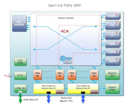
The NPU architecture is designed to enable scaling from a few GOPS to multiple TOPS, and it allows multi-island configurations for extensive optimization, including voltage and frequency scaling to optimize power consumption. It also permits multi-model computing that assigns models such as movement recognition or low-demand networking tasks flexibly according to workload and criticality.
Although more powerful, and well adapted to tiny edge AI, NPUs integrated in microcontrollers must work with extremely limited resources. Maximizing local data reuse is a priority and maintaining a balance between compute performance, routing, and interface bandwidth is vital. A deficiency in any one of these, relative to the others, creates a bottleneck that limits system performance.
Based on currently available 40-, 28-, and 18-nm FDSOI, and 16-nm FinFET fabrication technologies, neural processing benchmarks are projected to reach 1 to 5 TOPS/W and 0.1 to 2 TOPS/mm2 with NPU acceleration alone. These metrics also depend on NPU architecture and application operating modes.
However, anticipated market demands call for performance and efficiency rising to 50 to 200 TOPS/W over the next five years. Scaling NPU performance requires adding hardware, though, such as extra processing blocks and broader interconnects that increase silicon area and power. A different approach is needed.
Embedded In-Memory Compute
Despite the different computational principles at the heart of neural processing, the underlying hardware behavior is the same as that of traditional systems. Although the NPU establishes parallelism through many small sequential units, memory remains passive and executing instructions in the processing unit requires bringing data across an interface of strictly limited bandwidth.
In-memory compute (IMC) is a promising technique in high-performance computing and is extremely well-suited to linear operations like vector multiplications in neural processing. Developing IMC for edge platforms can potentially deliver the large gains in power efficiency and computing density in terms of TOPS/W and TOPS/mm2 of silicon needed to meet future expectations for edge AI performance (Fig. 2).
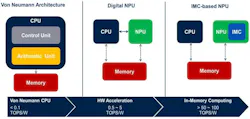
There’s more than one way to realize IMC and the technique is at the beginning of its development cycle. Digital IMC (DIMC) implements multipliers inside memory. In analog IMC, the network weights are encoded in memory cell states and multiplications are performed in situ based on analog phenomena such as Kirchhoff’s law or Ohm’s law.
Digital IMC
Digital IMC is typically implemented with SRAM arrays, holding weights, or small tensors that are tightly coupled with fixed-function logic such as MAC units fabricated locally. DIMC tiles are the internal combined temporary storage and computing workhorses of this new type of NPU. The compiler handles assigning operations to the NPU and its internal IMC block orchestrates data movement between them.
The internal DIMC tiles are small, and weights are reloaded for each computation. By making it possible to handle arbitrary complex neural networks like transformers and recurrent neural networks, or RNNs (including GRUs, LSTMs), as well as enhancing the performance of convolutional neural networks (CNNs) typically used for computer vision, DIMC can extend edge AI use cases to encompass new opportunities such as time-series analysis.
However, digital IMC still calls for moving data and is subject to memory bandwidth limits and clock-related throughput limitations. The area cost of digital multipliers must also be considered.
Analog IMC
Analog IMC is appropriate to SRAM or embedded non-volatile memory (eNVM), including charge-based flash or resistance-based types such as phase-change (PCM) and ferroelectric (FRAM) memories (Fig. 3). Weights are stored in the charge state or conductance state of the cells; outputs are summed as currents; and a matrix-vector multiply can be performed in one shot when the cells are activated.
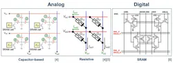
As this is analog electronics, signals need time to settle and the results can be affected by factors such as noise and temperature drift, which requires compensation.
IMC eliminates the memory-interface bottleneck and delivers parallelism without area cost. In analog IMC, the memory array is effectively the compute unit — no digital engine is needed. Reducing compute energy by orders of magnitude compared to conventional processor-memory interaction makes power efficiency a strong point, and high-density multi-level storage is possible. Meanwhile, tile size determines application-mapping efficiency as larger tile sizes can boost TOPS/W at the expense of lower area utilization. Though digital IMC is less dense, very large networks can be handled as weights and quickly reloaded in SRAM.
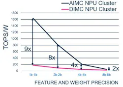
Each technique has its strengths, and committing to develop both gives edge-AI developers the flexibility they need to create properly optimized solutions. Figure 4 compares the acceleration, efficiency, and precision of digital and analog IMC.
Performance Enhancement Potential
Application developers and chip vendors understand that software alone, running on conventional MCU architectures or even MCUs enhanced with neural accelerators, can’t deliver the performance progression needed to meet future edge AI processing requirements.
Digital IMC and, ultimately, analog IMC that relieves both data movement and the propagation delay associated with digital processing, show the way forward for neural processing on resource-constrained embedded MCUs. Ultimately, edge AI energy efficiency could improve up to 100X (Fig. 5).
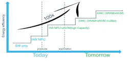
IMC design is implicitly connected with array size and shape, memory technology, routing, and hardware placement. By effectively migrating compute into device physics, IMC connects with the silicon layout in a way unlike previous hardware accelerators. The silicon defines the computation. The compiler can handle mapping the model onto the available fabric and orchestrating the available resources.
Viewed from this standpoint, ST’s proprietary Neural-ART Accelerator is an example of the process-level control and flexibility needed to embed effective IMC acceleration in future generations of edge AI microcontrollers.
Conclusion
The embedded NPU is already becoming an essential tool driving the performance of edge AI forward to meet the needs of future applications. However, further acceleration is needed, beyond the potential of today’s NPUs alone. In addition to raw compute speed, both energy efficiency, in TOPS/W, and area efficiency in TOPS/mm2 are the dominant performance metrics.
IMC overcomes memory bandwidth limits by performing the computation inside the array at the location of the data, and as the data is accessed. Only the computation result leaves the array.
Both digital and analog IMC are viable and effective strategies to continue accelerating neural processing at the edge. For MCU vendors, control over the NPU architecture as well as the fabrication technology is critical to realize these accelerators and deliver the tools that developers will need to fulfill their potential.
About the Author
Edwin Hilkens
STM32 Product Marketing Manager, STMicroelectronics
Edwin Hilkens is STM32 Product Marketing Manager at STMicroelectronics. He earned a Master degree from Hasselt University.
François de Rochebouët
Head of AI Solution Marketing, STMicroelectronics
François de Rochebouët heads the AI Solution marketing group at STMicroelectronics.
Related
 Leaders Logo
Leaders relevant to this article: