Materials Pave Way To Military Advances
Technological progress provides a military edge, regardless of whether those new technologies benefit forces on land, at sea, or in the air. RF/microwave technology, which has long been associated with a wide range of defense-related systems—including radar, secure communications, and electronic-warfare (EW) systems—might seem mature. But work is always moving forward on the “building blocks” of RF/microwave circuits and systems: electronic materials. Advances in numerous high-frequency electronic materials, including gallium nitride (GaN) and graphene, are promising to bring higher levels of RF/microwave performance and reliability to the battlefield.
GaN transistors and amplifiers based on those devices have been touted for some time as replacements for more mature traveling-wave-tube (TWT) vacuum-device technology. Due to limitations in output power for gallium arsenide (GaAs) field-effect transistors (FETs) and in upper frequency limit for silicon bipolar transistors, those device technologies have never challenged the high-frequency, high-power position of TWTs and TWT amplifiers (TWTAs) in military electronics systems. But with enhanced output-power performance due to GaN’s high electric-breakdown-field properties, its high saturated electron drift velocity, and its high thermal conductivity, this semiconductor material offers tremendous potential not only for achieving higher microwave frequencies, but for providing “tube-like” output-power levels at those frequencies. (For more on power-handling capabilities of different materials, click here.)
When in need of technology improvements, the US Department of Defense (DoD) tends to work through its research arm, the Defense Advanced Projects Research Agency (DARPA; www.darpa.mil). DARPA has been involved in the pursuit of practical GaN transistors and amplifiers through its Nitride Electronic Next-Generation Technology (NEXT) program, which is nominally aimed at developing devices with cutoff frequencies in the THz range, for use in linear mixers, power amplifiers, and power data converters.
One major opportunity for GaN technology is for the transmit portion of the US Navy’s Next-Generation Jammer (NGJ) platform. This is the first new electronic jamming system since the existing ALQ-99 jammer was installed in EA-6B Prowlers. The Prowlers were eventually replaced by EA-18G Growler aircraft, but not the jamming system. As a result, the Navy has issued a request for proposal (RFP) for a totally new system (the NGJ) which will likely employ GaN-based solid-state power amplifiers for transmission.
The existing ALQ-99 jammers have hardly kept pace with the rapid expansion of wireless communications technologies. They were developed during the early 1970s, before cellular telephones, frequency-hopping radios, and improvised explosive devices (IEDs). The ALQ-99 systems are limited in frequency coverage and output power, unable to combat simultaneous threats or to jam agile communications systems. The NJG systems will be designed for flexibility, since they must fit into a variety of dissimilar airframes with a modular, open-architecture design. The current ALQ-99 systems employ mechanically steered antennas to aim jamming signals. They will be replaced by electronically steered antennas. Many of the other, older technologies, such as signal sources and amplifiers, will be upgraded out of necessity, paving the way for direct-digital-synthesizer (DDS) signal sources and solid-state GaN amplifiers.
The Navy is looking to four industry stalwarts—BAE Systems, ITT Exelis, Northrop Grumman, and Raytheon—for a NGJ system solution. Whichever company wins the contract is sure to solicit solid-state power from one of a growing number of high-frequency component/subsystem suppliers. In support of the advanced technologies needed for the NGJ program, the Office of Naval Research (www.onr.navy.mil) has initiated itsNext-Generation Airborne Electronic Attack (NGAEA) program to encourage the development of such technologies as RF antenna arrays, RF power amplifiers, RF beam-forming networks, RF exciters (such as techniques and waveform generators), which will also be in support of Marine Corp airborne electronic-attack missions. These technologies will improve airborne electronic-attack capabilities across a broad range of missions, including suppression of enemy air defenses and denial of communications systems.
GaN device and amplifier technology is still in its early stages, but the semiconductor material provides great promise for improved efficiency and reliability and much smaller size and weight compared to TWTAs, especially at lower power levels and frequencies. Long-time amplifier supplier CTT, Inc. (www.cttinc.com), for example, now offers GaN solid-state amplifiers for industrial and military applications, notably as replacements for TWTAs in pulsed and continuous-wave (CW) applications from 2 to 18 GHz. For military programs, including radar and jamming systems, trying to comply with newer Size, Weight, and Power (SWaP) requirements, these GaN amplifiers can be supplied in extremely compact metal housings with coaxial connectors and automatic thermal shutdown to protect against damage from overheating.
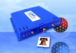
As an example of their broadband capability, model AGM/180-4550 provides 50-dB gain with ±3-dB gain flatness from 6 to 18 GHz. It delivers +45-dBm (32-W) CW output power with an 8-dB noise figure across operating temperatures from -55 to +85°C. It draws 8.8 A peak current from a +32-VDC supply. For narrowband applications, the firm’s model AGN/107-4957-P GaN power amplifier achieves 57-dB gain with ±2-dB gain flatness from 9.9 to 10.7 GHz. The compact amplifier (Fig. 1) generates +49-dBm CW output power and 80-W peak output power (with pulses to 100 μs and 10% duty cycle) with a 6-dB noise figure across the same operating temperature range. It draws 13.8-A peak current from a +30-VDC supply.
1. Model AGN/107-4957-P is an example of a high-power GaN amplifier in a modular housing for narrowband applications, from 9.9 to 10.7 GHz. [Photo courtesy of CTT, Inc. (www.cttinc.com).]
EMPOWER RF Systems (www.empowerrf.com) designs and builds both rack-mount GaN amplifier systems (see p. 100) and smaller modular GaN amplifiers for military applications through 6 GHz. As an example of their smaller amplifiers, model 1146-BBM4A6AK5 offers 40 W output power at 1-dB compression and as much as 100 W saturated output power, from 1 to 3 GHz, in a package measuring just 6.81 x 4.43 x 1.14 in. and weighing 2.2 lbs. The compact housing includes control, monitoring, and protection circuitry, can handle operating temperatures from -20 to +85°C, typical altitudes as high as 30,000 ft., and is screened to MIL-STD-810F for shock and vibration. The GaN amplifier yields 7-dB minimum power gain and 10-dB minimum small-signal gain, with +37 dBm input power needed to reach its rated output levels. It has a 10-dB noise figure and is quite linear, with a third-order intercept point (IP3) of typically +58 dBm. The amplifier draws 10 A from a +28-VDC supply.
In addition to competing with TWTs for signal-amplification chores across military airspaces, GaN amplifiers, because of their smaller sizes, will play increasingly important roles in the transmit sections of communications systems in small unmanned aerial vehicles (UAVs). NuWaves Engineering (www.nuwaves-ltd.com) is one of a growing number of companies offering GaN amplifiers for that purpose. The company’s model NW-SSPA-MICRO-5W-1.0-2.5 power amplifier provides 5 W typical RF output power across L and S-band frequencies from 1.0 to 2.5 GHz with 37-dB small-signal gain and better than 35% efficiency, all from a package measuring just 1.8 x 1.8 x 0.4 in., not including the additional heatsink. It is designed for operating temperatures from -30 to +70°C and draws 0.8 A typical current from a +28 VDC supply.
GaN technology has enabled Aethercomm (www.aethercomm.com) to miniaturize its model SSPA 7.6-7.8-150 solid-state amplifier while providing considerably more power than possible from conventional GaAs FET devices. It measures just 4.85 x 7.95 x 1.42 in. but delivers more than 150 W typical output power from 7.6 to 7.8 GHz for use in military ground vehicles. It features ±0.5-dB output-power flatness across the band and is designed for use with a +18 to +36 VDC vehicular power supply and at operating temperatures from -40 to +85°C. It is equipped with DC switching circuitry that enables and disables the RF devices in only 4 {LC MU}s for turn-on time and typically 500 ns for turn-off time. It also includes reverse polarity protection and open- and short-circuit protection.
Not all slots for GaN amplifiers are in military systems. Companies such as RFMD (www.rfmd.com) have seen healthy growth for their lower-power GaN amplifiers in cable-television (CATV) applications. Canadian satellite-communications (satcom) equipment supplier Advantech Wireless (www.advantechwireless.com) is aggressively comparing its new GaN satcom amplifiers and combination block upconverters (BUCs) to components based on silicon LDMOS and GaAs FET devices; the firm is claiming as much as 70% less power consumption and as much as 30% less heat generation for GaN equipment, in enclosures that are a fraction of the size. The company recently published a white paper (available on their website) on the merits of GaN technology for satcom applications, and throughout the month of September offered $1000 off the price of a new GaN power amplifier for any customer willing to trade in their old satcom TWTA.
Optimism surrounding GaN is so strong, that it was a year in which silicon LDMOS stalwart Freescale Semiconductor (www.freescale.com) introduced their first GaN amplifier, model AFG25HW355S, with volume availability later in 2013. Designed into a flange-type package, the GaN device is designed to deliver 350 W peak output power from 2.3 to 2.7 GHz. It includes target specifications of 16-dB gain and 50% efficiency, with nominal applications targeting cellular and wireless-communications markets.
Yet, in spite of this excitement surrounding GaN transistors and amplifiers from military and even commercial satcom and wireless-communications technology forecasters, some suppliers of TWTAs are seeing strong demands for their products. These include dB Control (www.dbcontrol.com) and e2V (www.e2v.com; click here for more). Some companies, such as Teledyne Microwave (www.teledynemicrowave.com), which also makes TWTs and TWTAs, support a number of different solid-state device technologies for RF/microwave power amplifiers, including GaN.
At higher frequencies, a carbon-based material has sparked the interest of military technology researchers: graphene. This is essentially a single layer of carbon atoms densely packed in a honeycomb crystalline lattice configuration. The material is an almost ideal semiconductor substrate, with high current-carrying capability, excellent thermal conductivity, and very high mobility through the material, which supports higher frequency operation. In fact, the transport capability of graphene is higher than any known semiconductor material at room temperature, with the speed of current materials limited only by impurities in the material.
Scientists at HRL Laboratories (www.hrl.com) recently demonstrated the world’s first graphene-based millimeter-wave square-law detectors with a linear dynamic range exceeding 60 dB. Using typical test frequencies at 170 and 214 GHz, these graphene FET detectors outperformed the best currently available silicon CMOS or silicon-germanium (SiGe) bipolar detectors by more than 30 dB in their linear range. The performance capabilities of these devices and this material could lead to impressive new capabilities in high-bandwidth communications, imaging, and radar systems.
Formerly Hughes Research Labs, HRL Laboratories boasts a rich history of innovation. The organization now serves as a research arm for and owned by The Boeing Co. (www.boeing.com) and General Motors (www.gm.com), and is performing its graphene investigations under the sponsorship of DARPA’s Carbon Electronics for RF Applications (CERA) program and under the management of the US Navy’s Space and Naval Warfare Systems Center (SPAWAR; San Diego, CA). HRL, which produced the first graphene-based transistors in 2008, is collaborating with numerous universities as well as with Naval Research Laboratory (NRL) to explore the performance possibilities of this novel semiconductor material. HRL Laboratories, which also has developed millimeter-wave GaN-based devices, has made these devices available to commercial customers.
HRL will attempt to deposit a layer of graphene carbon crystals on silicon wafers, making high-frequency devices that are scalable and more cost-effective to produce. The researchers will use a carbon molecular-beam-epitaxial (MBE) process developed by HRL to deposit a single-crystal layer of graphene onto a silicon substrate. The research is next projected to produce devices on 100-mm wafers, and then scaling the work to fabricate devices on 200-mm wafers.
Meanwhile the US Army Research Laboratory (ARL; www.arl.army.mil), in particular the Sensors and Electron Devices Directorate (SEDD), has entered into a three-year agreement with the Electronic Materials Research Institute at Northeastern University (Boston, MA; www.northeastern.edu) to develop graphene-based technology for low-cost infrared (IR) imaging applications for the military. Part of the project, which is also in collaboration with DARPA, is to produce graphene-based bolometers to measure heat from objects or personnel. These graphene bolometers may be used in night-vision goggles or for thermal body imaging. A longer-term goal is to license and mass-produce the technology for use in low-cost IR cameras.
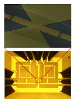
Of course, any discussion of graphene should include IBM (www.ibm.com). More than a year ago (and also with modest funding from DARPA), IBM fabricated the first graphene-based integrated circuit (IC), an RF mixer capable of operating to 10 GHz, nominally for secure military communications systems (Fig. 2). The graphene layer was deposited on a silicon wafer as the base. In addition to graphene’s electrical qualities, IBM has also been exploring its optical properties, using multiple layers of graphene in a graphene/insulator superlattice that supports devices at terahertz frequencies.
2. IBM’s work on developing graphene as a semiconductor material has included the fabrication of the first IC, a mixer capable of operating to 10 GHz. [Photo courtesy of IBM (www.ibm.com).]
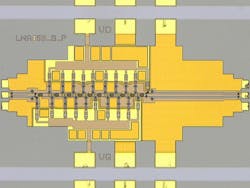
DARPA has strong interest in THz frequencies as part of its THz Electronics program, which has already demonstrated 0.85-THz radio capability as part of its quest for electronic circuits capable of THz operation, demonstrating receiver gain in an IC fabricated at that frequency (Fig. 3). The agency hopes to use these higher frequencies for advanced communications and sensor systems in support of DARPA’s Video Synthetic Aperture Radar (ViSAR) program. The ViSAR project is attempting to develop a targeting sensor capable of operating effectively through clouds.
3. This receiver IC has demonstrated gain at 0.85 GHz, as part of a program to produce ICs operating above 1 THz. [Photo courtesy of DARPA (www.darpa.mil).]
Both GaN and graphene hold great promise for military electronics systems, with GaN somewhat closer to its potential than graphene. GaN represents a more conventional semiconductor process, with impressive large-signal capabilities, while graphene may one day pave the way for low-cost communications at millimeter-wave frequencies and beyond.
About the Author
Jack Browne
Technical Contributor
Jack Browne, Technical Contributor, has worked in technical publishing for over 30 years. He managed the content and production of three technical journals while at the American Institute of Physics, including Medical Physics and the Journal of Vacuum Science & Technology. He has been a Publisher and Editor for Penton Media, started the firm’s Wireless Symposium & Exhibition trade show in 1993, and currently serves as Technical Contributor for that company's Microwaves & RF magazine. Browne, who holds a BS in Mathematics from City College of New York and BA degrees in English and Philosophy from Fordham University, is a member of the IEEE.


