Invisible, Integrated, and Intentional: Transparent Antennas in Modern Device Design
What you'll learn:
- How transparent antennas improve device design by freeing space and enhancing aesthetics without sacrificing performance.
- Why additive manufacturing outperforms chemical etching for creating high-precision, sustainable antenna structures.
- Where transparent antennas are being adopted today, from NFC smart cards to AR/VR devices and automotive glass.

High-transparency antennas began life as a cosmetic feature. However, they’re now seeing acceptance as an important design option for a wide range of products that have display screens, encompassing everything from smartphones to motor vehicles.
Some early applications of transparent antennas are taking advantage of the aesthetics of their virtual invisibility to the naked eye. Being able to hide an antenna in plain sight gives designers some spatial freedom in its placement, making room for other electronics or a larger battery.
A New Frontier for Antenna Design
Recent applications for transparent antennas include those in the NFC-enabled smart card sector. Typically, smart cards use wire-wound antennas made of small-diameter wire. While some end users like these visible antennas for their “cool factor,” many card manufacturers have sought to hide them completely for aesthetic reasons. Card designers utilize methods like card graphics, coloring, metal conductor treatment, or translucent overlays to help hide the antennas.
Though these transparent antenna card designs may have a certain uniqueness or differentiation, the antenna pattern often clashes with the overall graphics and overlays of the product. This has been a long-standing design challenge for card manufacturers to overcome. To address this issue, TDK has focused on balancing transparency and antenna performance.
The Core Challenge: Seeing Less Without Losing Signal
A common method for manufacturing transparent or nearly transparent antennas relies on creating them through a chemical etching process that begins with a solid sheet of copper. The base metal is removed from the areas where it’s not needed. While effective, this approach is highly wasteful and comes with several drawbacks.
One major issue with chemical etching is controlling the geometry of the metal traces. The process doesn’t produce straight, vertical walls, but rather ends up with a shape where the top of the trace is thinner than the bottom. Such a pyramid-like shape results from the upper side of the copper being exposed to the chemical for a longer period. This non-optimized metal cross-sectional area then increases the antenna’s resistance and thus, the performance can be reduced.
Another challenge lies in the gap between adjacent metal traces. Antenna designers must design for worst-case scenarios by planning for a larger-than-optimal gap between traces.
>>Download the PDF of this article, and check out the TechXchange for similarly themed articles and videos


Chemical etching works, but it limits antenna manufacturers’ control over the initial metal thickness. Thus, any design changes requiring a different metal antenna thickness may mean ordering new sheet stock, hindering iterative improvements.
What’s more, using chemical etching to produce the antenna is a subtractive process that’s both inefficient and wasteful. Yes, most of the etched copper can be retrieved, but then it must be reprocessed, costing time, effort, and money.
An alternative is to use an additive process that places copper only where it’s needed. Not only is this approach more sustainable, eliminating material waste, it improves quality by enabling a more uniform copper trace for better antenna performance.
Additive Manufacturing: A Transparent Breakthrough
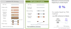
Unlike the subtractive etching process, TDK’s method involves an additive-pattern-coil plating process centered on copper electroplating deposition, resulting in zero copper waste (Fig. 1). With 17 years of using the process in power inductors and six more in wireless charging coils, it has lately been applied to NFC-based smart cards. Apart from the sustainable aspects of this process, it offers several technical advantages.
This additive process begins with applying a proprietary resin to the PET film substrate to ensure that the copper sticks only to the desired areas. The electroplating process is a tightly controlled, accurate multi-step process, which yields a uniform trace pattern and shape. Though this process can seem painstaking, it allows for narrower gaps between the adjacent traces and improves the copper cross-sectional area.
For transparent antennas in smart cards, which require a single-sided design, this process is particularly advantageous. The resin can also be used as a blackening layer to reduce antenna visibility by changing the hue, tone, tint, and/or shade, as well as reducing the copper’s luster. And, if so desired, the transparent antenna can be attached to an optically clear adhesive (OCA) or other adhesive materials and removed from the PET carrier film.
Tunable and Transparent NFC Cards
In contrast to conventional subtractive chemical etching processes, an electroplating process isn’t limited by the fixed thickness of copper sheets. The additive process enables full control of copper thickness, which allows for on-the-fly adjustments to address performance issues, such as reducing both DC and AC resistances, without the delays and cost of starting over with new copper sheets.
The fine pitch control of the additive-pattern-coil electroplating process makes it possible to create any antenna design to meet specific performance or transparency requirements. The first-generation process, which is ready for mass production, can create copper traces as fine as 30 µm, with pitch traces starting at 80 µm and scaling upward, and copper trace heights of between 1 and 5 µm.
The advanced second-generation process, called nano in-print, uses an ultra-thin, UV-resin-based mold/template to create the copper traces in fully customizable one-sided copper antenna patterns. The solid mesh or loop pattern now has a typical trace width of 2 µm with minimum trace pitches of 50 µm and heights of 3 µm or less.
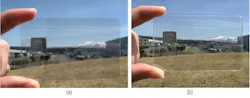
The transparency improvement of the NFC card antenna over the first-generation process is shown in Figure 2. As pictured, the card on the left (Fig. 2a) uses the first-generation process, where one can observe the uniform patterning and color for a full mesh antenna configuration. The card shown on the right (Fig. 2b) utilizes the second-generation process. It provides a solution with much lower haze, which can easily be seen by looking at Mount Chokai in the background.
For NFC smart cards, industry standards from bodies such as EMVCo mandate a 40-mm read range for contactless cards using both direct connection and magnetic coupling. Achieving that 40-mm range may dictate employing some design “tricks.”
For example, when it comes to full-mesh antenna patterns, this means directing the current into the smart chip’s coil area to create an optimized magnetic field that activates the smart chip. For loop antenna patterns, designers may need resonant capacitors to tune the antenna to the desired 13.56-MHz frequency.
Beyond Cards: Broader Implications for Transparent Antennas
A combination of aesthetic desires and the practical space constraints in modern electronic devices is driving innovation in industrial design. For smart devices, connectivity to networks like cellular, Wi-Fi, Bluetooth, and more necessitates an antenna.
Looking beyond NFC cards, transparent antennas hold significant potential in augmented- and virtual-reality (AR/VR) applications. For instance, mounting these antennas on the glass surface of a pair of AR/VR glasses is a practical and innovative solution. When positioned close to the eye, these transparent antennas become nearly invisible.
Currently, for cell phones and smart watches, the antenna is often integrated into the side of the case, taking up valuable space. Positioning an optically transparent antenna above the display or even integrated within the display system itself would free up space for additional electronics or a larger battery.
Similar on-glass or in-glass applications exist in the automotive space. Transparent antennas have been integrated with automotive windows for various RF technologies, including cellular, Wi-Fi, and GNSS, for many years.
These applications have had to deal with the tradeoffs between transparency and the antenna’s resistance for performance. If placed in the windshield, antennas have been hidden in the upper tinted areas in the past, meaning high transparency wasn’t the driving factor and the focus shifted more to the resistance value.
However, there’s a fundamental tradeoff between antenna performance and its transparency. Increasing the pitch between traces and decreasing the trace widths in the mesh pattern makes the design more transparent, but in most cases, leads to a decrease in performance. The importance of this balance depends on the application. For example, antenna transparency might be less critical in the tinted area of that car’s windshield compared to a cellphone display.
Another non-antenna use for the mesh copper patterning has involved EMI protection. Metal mesh screens are manufactured the same as the antennas. In the automotive sector, this means EMI protection for information displays (e.g., GPS devices), in center-console wireless power chargers, and possibly internal mirrors with integrated electronics.
In addition, for both automotive glass and mirrors, and for inner-vehicle displays, the same technology can be used to make transparent heaters for defrosting/defogging.
Key Takeaways and Future Outlook
Transparent antennas are no longer a novelty. They’re solving real integration challenges, especially in space-constrained, user-facing applications such as smart cards, AR/VR glasses, wearables, and automotive glass. The integration of transparent antennas in these devices offers a unique combination of aesthetic appeal and functional efficiency, making them standout solutions for next-generation technology.
Additive-manufacturing techniques, such as TDK’s electroplated pattern coil technology, enable thin, high-performing, and environmentally sustainable transparent antennas. Though transparency and antenna performance often involve tradeoffs, advances in fine patterning, blackening treatments, and antenna designs assist the end-product designers by offering newly created options. As transparency becomes a feature, expect further expansion into new domains.
>>Download the PDF of this article, and check out the TechXchange for similarly themed articles and videos
About the Author
Harvey Espinoza
Harvey Espinoza, Sr. Director of Product Marketing, TDK Corp.
Harvey Espinoza is Senior Director of Product Marketing at TDK Corp.
