Ceramic Substrate Shrinks Patch Antenna
Wireless electronic products continue to shrink in size, requiring ever-smaller antennas. To fill this need, the authors developed a three-stack wideband patch antenna on aluminum-oxide ceramic substrate material. The high relative dielectric constant of the substrate made it possible to reduce the dimensions of the antenna without compromising the performance of the component. The antenna was designed with the aid of commercial electromagnetic (EM) simulation software—namely, the High-Frequency Structure Simulator (HFSS) from Ansoft (www.ansys.com). This design targeted an operating frequency range of 16.20 to 19.31 GHz, achieving peak gain of 8.531 dBi with radiation efficiency of 84 to 89% and return loss of better than 10 dB across the operating bandwidth. The antenna was designed for Ku/K-band applications.
As wireless products are designed with increased functionality, antennas must provide broadband performance, but in smaller sizes. A great deal has been written about the use of high-dielectric-constant circuit materials to shrink high-frequency circuit dimensions.1 In addition, antenna designers have developed a variety of novel structures in attempts to achieve miniaturization. Patch antennas have long been used for many forms of communications and radar systems, as well as for GPS location systems.2
Patch antennas offer attractive performance for a wide range of wireless applications, but must be designed for small geometries to meet the demands of modern electronic devices. Numerous researchers have turned to high-dielectric-constant substrate materials to help miniaturize their antenna designs, as well as designs based on reactive impedance substrates, dielectric resonators, and magneto-dielectric substrates.3 Substrates based on dielectric ceramic materials are promising candidates for antenna miniaturization because of their high permittivity, low loss, light weight, low cost, and market availability.4
Attempts to miniaturize antennas have employed many different techniques, including the use of low-temperature co-fired-ceramic (LTCC) substrates,5 planar monopole ring antenna designs using FR-4 substrate,6 the use of ceramic material for a proximity-coupled feeding structure,7 EM bandgap-based planar ceramic antennas,8 and even substrates based on artificial magnetic materials and fractal Hilbert curves to increase the effective permeability.9 However, most of the antennas produced by these techniques are relatively large in size, with low gain, low efficiency, and/or narrow bandwidths. There is still much room to explore the possibilities of using specific material substrates to aid antenna miniaturization.
The current work involves the design and fabrication of a three-stack patch antenna with coaxial probe feed, designed on Al2O3 ceramic material substrate. The antenna was analyzed using commercial EM software based on finite-element-method (FEM) analysis, the popular HFSS three-dimensional (3D) simulation software. The proposed patch antenna has a bandwidth of 3.11 GHz with 7.5-dBi gain at the resonant frequency of 17.20 GHz. The use of the Al2O3 ceramic material substrate and its high dielectric constant made it possible to shrink the dimensions of the patch antenna. The antenna was fabricated on 1-mm-thick Al2O3 ceramic material with relative dielectric constant of 9.8, relative permeability of 1, and ideal loss tangent of 0 when modeled without any conducting ground plane. The antenna can be designed on any nonconducting plane.
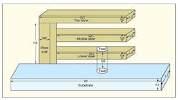
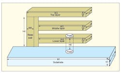
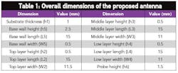
1. This diagram shows the basic geometry of the patch antenna on ceramic substrate, with the dimensions for a Ku/K-band design listed in Table 1.
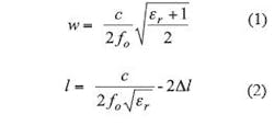
The design of the antenna starts with its radiating patch. The base wall of the patch was designed with 0.5-mm-thick copper in a stack of three sides lying along the Y-axis with a 0.5-mm gap between each stack. The geometry and design of the antenna are shown in Fig. 1, with the dimensions listed in Table 1. The dimensions were determined by mathematical model and customized according to Eqs. 1 and 210:
where:
w = the width of the radiating patch;
l = the length of the radiating patch;
f0 = the target center frequency of the patch; and
c = the speed of light in a vacuum.
By applying Eq. 3, the effective dielectric constant, εe, can be found10:
where:
h = the thickness of the substrate and
εr = the relative dielectric constant of the substrate.
Due to the fringing field around the periphery of the patch, the antenna electrically appears larger than its physical dimensions. The antenna was designed to operate from 16.20 to 19.31 GHz and optimized with HFSS for best performance across that bandwidth.
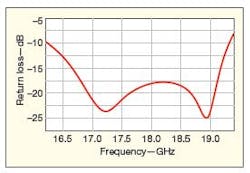
Figure 2 shows the return loss of the ceramic-based patch antenna, which is better than 10 dB in the desired frequency range. By changing the feed position 3 mm closer to the base wall, the lower resonance of the patch shifted from 17.2 GHz to 16.9 GHz. The antenna provides 1.8-GHz bandwidth at Ku-band frequencies and 1.31-GHz bandwidth for K-band applications.
2. The return loss of the patch antenna is plotted here as a function of frequency.
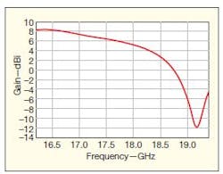
Figure 3 shows antenna gain as a function of frequency. The peak gain of 8.531 dBi occurs at 16.3 GHz where the radiation is more directional; the gain is 7.05 dBi at the resonant frequency of 17.20 GHz. Above 18.5 GHz, the gain declines sharply, with average gain of 3.5 dBi at those higher frequencies. The overall gain of the patch antenna can be increased by increasing the substrate thickness, but this will also impact the size of the antenna.
3. The patch antenna’s gain is shown here as a function of frequency.
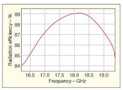
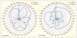
Figure 4 shows the overall radiation efficiency of the patch antenna, which ranges from 84% to 89% across the operating bandwidth. Figure 5 shows copolarization and cross-polarization radiation patterns in the electric (E) and magnetic (H) planes of the antenna at its resonant frequency of 17.20 GHz. The copolarization pattern is symmetric and more stable. The antenna provides stable, directional radiation patterns across its operating bandwidth.
4. The radiation efficiency of the ceramic-based patch antenna is plotted as a
function of frequency.
5. These plots show the radiation pattern of the patch antenna’s (a) E-plane response and (b) H-plane co-cross polarization response.
Figure 6 shows the current distribution of the antenna’s E-H field responses all along the radiating patch. From Fig. 6(a), it can be seen that the E-field current is stronger along the front side of the feed probe, as well as along the left, right, and back sides of the patch near the boundary line. The E-field current reaches its lowest point at the front side near the boundary line. The H-field current distribution in Fig. 6(a)is strong around the feed probe; it is weaker near the boundary line, as well as the left and right back corner sides. The current distribution can be improved by using other feeding techniques and positions. And finally, Table 2provides a comparison of this patch antenna with other efforts at miniaturizing high-frequency antennas.11-13 As it shows, the proposed antenna design is much smaller and exceeds the performance of the other antennas in the comparison.
6. These plots show the current distribution of the (a) E-field and (b) H-field patterns along the radiating patch.
M. HABIB ULLAH, Engineering Student, Institute of Space Science (ANGKASA), Universiti Kebangsaan Bangi Selangor, Malaysia 43600; e-mail: [email protected], e-mail: [email protected]. Department of Electrical, Electronic, and System Engineering, Faculty of Engineering and Built Environment, Universiti Kebangsaan, Malaysia
M.T. ISLAM, Researcher, Institute of Space Science (ANGKASA), Universiti Kebangsaan Bangi Selangor, Malaysia 43600
J.S. MANDEEP, Researcher, Institute of Space Science (ANGKASA), Universiti Kebangsaan Bangi Selangor, Malaysia 43600; Department of Electrical, Electronic, and System Engineering, Faculty of Engineering and Built Environment, Universiti Kebangsaan, Malaysia
References
1. M. Habib Ullah and M.T. Islam, "Design Of A Modified W-Shaped Patch Antenna On Al2O3 Ceramic Material Substrate For Ku-Band," Chalcogenide Letters, Vol. 9, No. 2, 2012, pp. 61-66.
2. Y.P. Zhang, C.W.Y. Ang, C.S.C. Lee, and M.A. Do, "Bandwidth Enhancement of A Patch Antenna of Very High Permittivity Materials," Microwave and Optical Technology Letters, Vol. 28, No. 2, 2001, pp. 98-99.
3. D.H. Schaubert, D.M. Pozar, and A. Adrian, "Effect of microstrip antenna substrate thickness and permittivity: comparison of theories with experiment," IEEE Transactions on Antennas & Propagation, Vol. 37, No. 6, 1989, pp. 677-682.
4. J.-C. Iriarte, I. Ederra, and R. Gonzalo, "Design and characterisation of a high efficiency ceramic ebg patch antenna," IET Microwave Antennas Propagation, Vol. 4, No. 8, 2010, pp. 1056-1062.
5. J.S. Kula, D. Psychoudakis, W.-J. Liao, C.-C. Chen, J.L. Volakis, and J.W. Halloran, "Patch-antenna miniaturization using recently available ceramic substrates," IEEE Antennas & Propagation M, Vol. 48, No. 6, 2006, pp. 13-20, 2006.
6. Rezaul Azim, Mohammad Tariqul Islam, and Norbahiah Misran, "Printed Planar Antenna for Wideband Applications," Journal of Infrared, Millimeter, and Terahertz Waves, Vol. 31, No. 8, 2010, pp. 969-978.
7. J.-S. Kim, W.-K. Choi, and G.-Y. Choi, "Small proximity coupled ceramic patch antenna for UHF RFID tag mountable on metallic objects," Progress In Electromagnetics Research C, Vol. 4, 2008, pp. 129-138.
8. L. Yousefi and O.M. Ramahi, "Miniaturized antennas using artificial magnetic materials with fractal Hilbert inclusions," Electronics Letters, Vol. 46, 2010, pp. 816-817.
9. R. Azim, M.T. Islam, and N. Misran, "Compact Tapered Shape Slot Antenna for UWB Applications," IEEE Antennas & Wireless Propagation, Vol. 10, 2011, pp. 1190-1193.
10. R. Azim, M.T. Islam, and N. Misran, "Dual Polarized Microstrip Patch Antenna for Ku-Band Application," Inform MIDEM, Vol. 41, 2011, pp. 114-117.
11. R. Azim, M.T. Islam and N. Misran, "A Planar Monopole Antenna for UWB Applications," International Review of Electronic Engineering, Vol. 5, No. 4, 2010, pp. 1848-1852.
12. A.R. El-Damak, H. Ghali, and H.F. Ragaie, "Wideband modified Sierpinski slot antenna," IEEE Antennas and Propagation Society International Symposium, Vol. 2B, 2005, pp. 548-551.
13. A.U. Bhobe, C.L. Holloway, M.Piket-May, and R. Hall, "Coplanar waveguide fed wideband slot antenna," Electronics Letters, Vol. 36, No. 16, 2000, pp.1340-1342.
