Exploring Virtual Crystal-Based 22-GHz RF Synthesizers

This article is part of the special report below.

What you’ll learn:
- Integer-N PLLs are smaller, better, cheaper, and faster, but they have poor frequency resolution.
- Ultra-low-jitter, multi-GHz, fully programmable frequency references are now available and can be used with integer-N PLLs for high-performance RF frequency synthesis: 22 fs at 22 GHz.
- What is a Virtual Crystal?
Frequency synthesizers provide the precise and tunable frequency sources required for modulation, demodulation, carrier generation, and channel selection in modern radio, wireless, and telecommunication systems. Among the various frequency synthesis techniques available, the phase-locked loop (PLL) is the most widely adopted due to its versatility, compact implementation, and ability to deliver both frequency accuracy and spectral purity across a wide range of applications.
At a fundamental level, a PLL is a closed-loop feedback system that generates an output frequency by multiplying a stable, low-frequency fixed reference signal (Fref) by a programmable ratio (N). The multiplication process guarantees that the output inherits the stability and accuracy of the reference while extending its frequency into the operational range required by the system.
As shown conceptually in Figure 1, a conventional PLL consists of four principal components:
- Phase-frequency detector and charge pump (PFD/CP): Detects the phase and frequency difference between the reference and the divided feedback signal and converts this difference into a current signal.
- Loop filter: Processes and integrates the charge-pump current, producing a control voltage that governs the oscillator.
- Voltage-controlled oscillator (VCO): Generates the output signal, whose frequency is proportional to the applied control voltage.
- Feedback divider: Divides the VCO output by the ratio N so that it can be compared with the reference at the PFD.
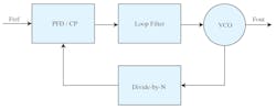
Through continuous feedback, the PLL synchronizes the phase and frequency of the output with the reference, effectively realizing a frequency synthesizer that combines accuracy with programmability.
Over the years, PLL architectures have evolved to balance the competing requirements of frequency resolution, spectral purity, noise performance, and implementation complexity. Two dominant architectures have emerged: the integer-N PLL and the fractional-N PLL.
The integer-N approach offers simplicity and inherently low phase noise, but it’s limited by coarse frequency resolution. Conversely, the fractional-N architecture provides fine frequency granularity and wideband agility, but it introduces additional design complexity and noise mechanisms that must be carefully managed.
Integer-N PLL
In an integer-N PLL, the feedback divider ratio, denoted as N, is restricted to integer values. For instance, if the objective is to generate an output frequency of 1 GHz from a Fref of 25 MHz, the required divider setting would be N = 40. The operational principle is straightforward: The PFD continuously compares the input reference clock against the divided version of the output clock and subsequently adjusts the phase of the VCO until the two signals are phase-aligned.
One of the primary advantages of the integer-N architecture is its inherent simplicity and low phase-noise performance. At lock, the PFD ideally produces no output activity, which translates into exceptionally low in-band phase noise. In addition, sub-sampling PFD (SSPD) techniques1 can further enhance noise performance when compared to conventional CP-based PLLs. This improvement arises because SSPDs mitigate both the divider-related noise and the N2 scaling of charge-pump noise, which typically degrade performance in CP implementations.
The primary limitation of the integer-N approach is its coarse frequency resolution. The minimum frequency step size is equal to the reference frequency, which constrains the granularity of frequency synthesis.
To achieve finer resolution, the reference frequency must be divided down prior to comparison in the PFD. However, this approach has a significant tradeoff, most notably that it reduces loop bandwidth. The result is slower dynamic response, longer settling times, and an increase in the effective division ratio N required to reach a given output frequency. Consequently, phase noise is amplified.
Fractional-N PLL
A fractional-N PLL extends the capabilities of the integer-N architecture by offering fine frequency resolution using a multi-modulus divider controlled by a delta-sigma (Σ-Δ) modulator. In contrast to the fixed integer divider of an integer-N PLL, the multi-modulus divider dynamically alternates between integer values under the control of the Σ-Δ modulator. Thus, the average division ratio can take on an effective division ratio of N+α, where α is the fractional part.
Such an approach allows the PLL to generate output frequencies in steps that are much smaller than the reference frequency, thereby providing agile tuning over wide frequency bands while still operating with a relatively high reference clock.
The ability to retain a fixed higher reference frequency offers an additional advantage: Fractional-N PLLs can support wider loop bandwidths, which in turn improves the suppression of VCO phase noise. This capability makes fractional-N PLLs especially attractive in fast frequency hopping or fine-grained channel-spacing applications.
However, these benefits come with significant tradeoffs in complexity and spectral purity. By design, the fractional-N architecture introduces quantization noise due to the Σ-Δ modulation process.
Because of the modulated division, the phase detector sees a reference and feedback that don’t align cycle-to-cycle. Instead, the instantaneous phase error “jumps” around, with the average phase error being driven to zero. Moreover, the periodic switching of the divider ratio, coupled with non-idealities in the charge pump and loop filter, gives rise to fractional spurious tones (fractional spurs) in the output spectrum.
While techniques such as Σ-Δ noise shaping, randomization, and calibration can mitigate the impact of these spurious components, they can’t be entirely eliminated. Consequently, fractional-N PLLs typically exhibit higher in-band phase noise and jitter compared to their integer-N counterparts, often with a degradation on the order of several decibels.
To manage these impairments, modern fractional-N implementations frequently incorporate spur-suppression circuits, including digital-to-time converters (DTCs) that linearize the phase updates2 introduced by the fractional divider. These techniques add cost, power consumption, and design overhead, and they further increase the architectural complexity of the system. As a result, fractional-N PLLs represent a tradeoff between the flexibility of fine frequency resolution and the challenges of maintaining low noise and high spectral purity.
Introducing the Virtual Crystal: An Ultra-Low-Jitter Programmable Frequency Reference
What if we could synthesize high-frequency clocks digitally, with the precision and flexibility of modern CMOS? Our answer is a new family of timing solutions built on a fully digital architecture. Our approach is built around the concept of a Virtual Crystal — a digitally synthesized, high-purity sine wave that replaces traditional quartz oscillators with a programmable, temperature-stable, and low-jitter reference.
This is how it works:
- A frequency control word (FCW) sets the desired frequency of the sine wave.
- A sine generator produces digital codewords of the waveform at the desired frequency.
- A high-performance DAC converts these codewords into analog voltages.
- A multi-GHz, temperature-stabilized, bulk-acoustic-wave (BAW), resonator-based oscillator provides ultra-stable timestamps to all circuits.
- A low-pass filter smooths the waveform, producing an ultra-low phase noise output.
This architecture replaces the entire analog oscillator/PLL chain with a mixed-signal CMOS block that can be integrated and configured using standard interfaces like I2C or SPI. The approach delivers sub-20 fs of jitter at multi-GHz frequencies and is fully programmable. These devices are standalone or configured as jitter attenuators/frequency translators.
Notable features of the virtual crystal-based oscillators and jitter attenuators include:
- Can lock to input frequencies up to 750 MHz (including 1 PPS, 10 MHz for jitter attenuation).
- Generate output frequencies up to 2 GHz (frequency translation).
- Deliver ultra-low jitter (as low as 19 fs RMS).
- ±20-ppm thermal stability (–40 to +105°C) as standalone references.
- Compact CMOS packages (as small as 2.0 × 1.6 mm).
- Programmable output frequencies: sub-Hz frequency resolution.
- Programmable phase.
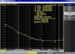
Figure 2 shows the phase noise of the Virtual Crystal reference at a frequency of 1.6 GHz. The measured RMS jitter, integrated from 12 kHz to 20 MHz, is 18.8 fs.
Who Needs a Fractional-N PLL?
To generate frequencies above 2 GHz, the Virtual Crystal may be combined with a commercially available integer-N PLL (Fig. 3). The commercial integer-N PLL accepts reference clocks under 500 MHz and generates output clocks up to 22 GHz.
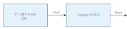
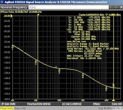
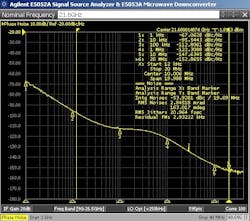
For any output frequency Fout, the Virtual Crystal is programmed to a frequency Fref such that Fout/Fref = N (an integer) and Fref < 500 MHz. Figures 4 and 5 show the measured phase noise at 8 GHz and 21.6 GHz. Both output frequencies have rms jitter less than 22 fs with an integration range of 12 kHz to 20 MHz. A closer look at the in-band phase noise suggests that it’s limited by the PFD of the integer-N PLL instead of the Virtual Crystal reference.
This approach offers multiple advantages:
- Because the Virtual Crystal reference frequency (Fref) can be programmed with sub-hertz resolution, the output frequency (N. Fref) can also be tuned in exceptionally fine steps. This addresses the coarse frequency-resolution limitation of integer-N PLLs. Thus, all the benefits of the integer-N PLL, including better performance and lower spurs, can be enjoyed without the need for a fractional-N PLL.
- A high-frequency reference reduces the required multiplication factor (N), thereby reducing output jitter. The loop bandwidth of the PLL can also be made wider, resulting in faster dynamic response and settling times.
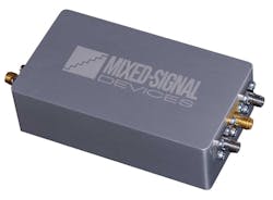
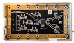
Mixed-Signal Devices recently set a new benchmark in RF performance with the MS4022 Frequency Synthesizer module (Figures 6 and 7). With output frequencies up to 22 GHz and ultra-low jitter of 22 fs RMS, the MS4022 is apt for next-generation radar, wireless infrastructure, phased array, and instrumentation systems.
The MS4022 also supports locking to external reference sources, e.g., OCXOs, GPS-disciplined oscillators (GPSDOs), and master clock trees, for precise synchronization with system-level timing requirements. It provides dual coherent outputs for phase-aligned signal-generation applications such as beamforming, MIMO, and multichannel instrumentation.
Furthermore, integrated jitter attenuation enhances performance by suppressing reference noise and guaranteeing exceptionally low phase noise. All of these capabilities support reliable integration into both standalone and distributed architectures.
Enhanced Synchronization
Multiple fractional-N PLLs sharing the same input reference clock don’t inherently guarantee a fixed or predictable phase relationship between their outputs, unlike integer-N PLLs. While each individual fractional-N PLL achieves a stable phase lock to its reference, the relative phase difference between the outputs of separate fractional-N PLLs can vary.
This lack of guaranteed phase coherence arises primarily from the nature of the ΣΔ modulators used in fractional-N PLLs. The SDM dynamically switches the division ratio of the feedback divider, allowing for fractional frequency synthesis.
The initial state of this SDM, along with the specific sequence of division ratio changes it generates, can influence the final output phase. If the ΣΔ modulators in multiple PLLs aren’t synchronized at startup or during operation, their outputs can settle to different, seemingly random, phase offsets relative to each other.
Achieving phase synchronization between multiple fractional-N PLLs requires additional synchronization mechanisms. This typically involves synchronizing the ΣΔ modulators themselves, often by ensuring they start from a known state or by using a common synchronization signal to align their internal operations. Without such measures, while the frequency of each PLL's output will be accurately controlled and locked to the reference, their relative phase alignment will be indeterminate.
A noteworthy characteristic of integer-N PLLs is the existence of a fixed phase offset between the input and output clocks. This property vastly simplifies the task of synchronizing multiple PLLs operating from the same reference source.
When all PLLs share a common reference, phase alignment across the system can be achieved with relative ease. Such an attribute is a boon for massive multiple-input multiple-output (MIMO) beamforming applications where coherent signal combining relies heavily on precise phase synchronization.
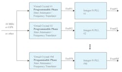
A Virtual Crystal jitter attenuator/frequency translator can lock on to an external reference (10 MHz or GPS) and generate a high frequency, low-jitter clock to multiple integer-N PLLs (Fig. 8). All output clocks are phase-aligned and synchronized with the low-frequency reference.
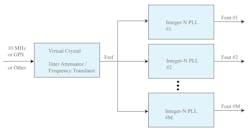
An alternative approach using multiple Virtual Crystals is shown in Figure 9. Since the phase of each Virtual Crystal can be programmed independently in very fine steps (32-bit resolution over the period of the clock), this allows for precise phase synchronization and adjustment over multiple integer-N PLLs. The phase of the Virtual Crystal can be programmed through an I2C/SPI interface.
Running the Reference at Higher Frequencies for Better Performance
It’s well known that a low-noise reference can improve the overall phase-noise performance of the PLL. For a fixed jitter spec, a 2X increase in reference frequency can reduce the VCO power by a factor of four, provided reference phase noises stay the same (Reference 3, Eq. 24).
For example, we compare a 156.25-MHz reference (−165 dBc/Hz at 4-MHz offset) and a 312.5-MHz reference (also at −165 dBc/Hz at 4-MHz offset). A 2X wider loop bandwidth can be used with 312.5 MHz to suppress a lower-power VCO with 6 dB higher phase noise.
A higher reference frequency can also help to suppress the phase noise from PFD/CP and reduce jitter. For instance, for a state-of-the-art commercially available PLL that has a normalized in-band phase noise of −239 dBc/Hz, the in-band phase noise with a 156.25-MHz reference is −157.1 dBc/Hz. For a 10-GHz output frequency, the in-band phase noise is −120.9 dBc/Hz. With a 625-MHz reference, the in-band phase noise for the same 10-GHz output frequency is −127 dBc/Hz or 1/2 jitter.
Summary
Virtual Crystal is a digitally synthesized, high-purity sine wave that generates a programmable, high-frequency, temperature-stable, and low-jitter reference. Higher frequencies and lower phase noise can result in better performance and/or lower power in the PLLs. The combination of Virtual Crystal and integer-N PLL is well-suited for the most demanding frequency synthesizer applications.
References
1. X. Gao et al., “A low noise sub-sampling PLL in which divider noise is eliminated and PD/CP noise is not multiplied by N2,” IEEE J. Solid-State Circuits, vol. 46, no. 11, pp. 2635-2649, Nov. 2009.
2. W. Wu et al., “A 14-nm ultra-low jitter fractional-N PLL using a DTC range reduction technique and a reconfigurable dual-core VCO,” IEEE J. Solid-State Circuits, vol. 56, no. 12, pp. 3756-3767, Dec. 2021.
3. B. Razavi, “Jitter-power trade-offs in PLLs,” IEEE Trans. Circuits Syst. I, Reg. Papers, vol. 68, no. 4, pp. 1381-1387, Apr. 2021.
Read more articles from this special report
About the Author
Tommy Yu
CTO and Founder, Mixed-Signal Devices
Dr. Tommy Yu, CTO and founder of Mixed-Signal Devices, has over 25 years of experience in the field of communication system architecture and circuit design. Prior to starting Mixed-Signal Devices, he was a technical director at Entropic Communication where he was the project lead for the digital satellite outdoor unit and cable front end products. Dr. Yu joined Entropic through the acquisition of Mobius Semiconductor where he was the director of system engineering. At Mobius, he developed the lowest power satellite outdoor unit and cable front end products in the industry.
Prior to joining Mobius Semiconductor, Dr. Yu was a senior principal scientist at Broadcom Broadband VLSI group. He was the system lead responsible for all satellite receiver products development at Broadcom and one of the key members that help to grow the satellite product revenue exceeds $500M.
Dr. Yu has 36 issued patents and 15 patents pending in the area of communication system and circuit design. Dr. Tommy Yu received B.S. (summa cum laude), M.S., and Ph.D. in Electrical Engineering from the University of California, Los Angeles.
