What is the 12-Term VNA Calibration Model?
This article is part of the TechXchange: Vector Network Analyzers.
Members can download this article in PDF format.
What you’ll learn:
- What are the error terms in the 12-term error model?
- How are these errors related to the simpler 8-term model?
- How is 1-port calibration performed?
- How are the error terms evaluated using calibration standards?
This is the third in a multi-part series of articles on vector network analysis. Part 1 introduced the VNA, how such instruments work, and some of their applications in the lab. Part 2 introduced S-parameter network flow diagrams and how to manipulate them to solve real-world problems.
Because test cables experience loss and delay, vector network analyzers (VNAs) must be calibrated to make precise measurements. Those cable losses mean that phase measurements made at the VNA ports will not be the same as those made at the device under test (DUT).
If the characteristic impedances of the test cables are not precisely 50 Ω, the effective source and load match of the VNA will be slightly off, resulting in measurement ripple. In addition, the directivity error in the VNA measurement bridges must be corrected to ensure accurate reflection measurements. This short primer will quantify the various systematic errors and introduce the 12-term error-correction model, which serves as a basis for VNA calibration.
The S-parameter network diagrams, as seen in the previous article in this series, will be used to describe the various error terms.
What is the 12-Term Error Model?
Our model starts with a perfect VNA. We create two error boxes and put them on either side of the DUT and attach the perfect VNA to the left and right sides of Figure 1.
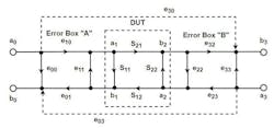
Error box A is defined by its four S-parameters—e00, e01, e10, e11—and error box B by S-parameters e22, e23, e32, and e33. The DUT is defined by its S-parameters S11, S12, S21, and S22. The S-parameters measured by the perfect VNA attached to the system, Sm, are altered by error boxes A and B. The isolation terms e30 and e03 are usually small and may be ignored for the moment.
The measured S-parameters, Sm, may be expressed as in Equation 1:

where Sa are the actual S-parameters of the DUT.
Unfortunately, you can’t multiply S-parameters as shown in Equation 1, but you can recast them as cascade (or transfer) parameters, and then matrix multiplication is valid. The conversion to cascade parameters is accomplished with Equations 2, 3, and 4:


where:


Then:

And we can find TDUT by inverting TA and TB:

We then convert the cascade parameters back to S-parameters, and we will have our calibrated measurement assuming we know the eight e values:

where the T parameters are TDUT from above. And:

The e values for the A and B boxes can be determined by making a few measurements of known calibration standards such as an Open, a Short, a Load, and a Thru.
But this is an 8-term error model, and the individual error terms don’t correspond well to any physical error contributor. The 8-term model can be modified into two 6-term models—one for each measurement direction—where the stimulus is emitted by Port 1 and received on Port 2 or the other way around. The error terms in this model relate to actual physical phenomena.
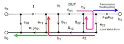
Referring to Figure 2, for a forward 6-term model, we can normalize e10 to 1. In doing so, any signal that comes back through e01 had to pass through e10 first, so we change e01 to e10e01. The same is true for e32, so we changed it to e10e32.
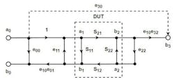
Lastly, we eliminated node a3 in the forward model because there’s no driven signal on the right side to feed it. With a3 gone, e33 and e23 go with it and we have Figure 2 with six error terms. Similarly, the reverse model is shown in Figure 3.
Focusing on the forward model, we can name these errors based on physical causes. a0 is the driven node and, ignoring isolation term e30 for now, the input signal from a0 immediately sees e00, which sends a signal right back to b0.
This is the directivity error, the signal that leaks from the incident signal into the reflection port of the directional bridge. The remaining forward traveling signal then encounters S11 of the DUT, generating a reflection, which heads back to the source.
That reflection encounters e11, the source-match error. The source-match error is seen right at the end of the test cable and is caused by any deviation from 50 Ω due to the cable, the connectors, and to some extent, the raw source-match error of the VNA itself. This source-match reflection is pushed back up to the top of the network diagram and reenters the DUT along with the incident signal.
The remaining S11 reflection, that which was not diverted by e11, passes through e10e01, the reflection tracking error. The reflection tracking error is essentially the frequency response of the test cable, the connectors (twice), and the internal hardware of the VNA in the reflection path of the measurement bridge. This error will be a gentle low-pass response, as the test cable will always be more lossy at higher frequencies. These first three reflections are shown in Figure 4.
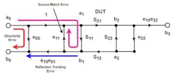
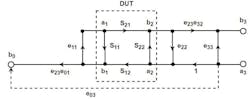
That part of the incident signal not reflected by the directivity error, or S11 of the DUT, enters the DUT and is affected by S21. This modified signal then sees e22, the load-match error, passes to the bottom of the diagram, and heads back toward a2. The load-match error is seen at the end of the test cable and is caused by any deviation from 50 Ω due to the cable, the connectors, and the raw load match of the VNA itself.
Some of that reflected signal at a2 is reflected upward again by S22 and rejoins the incident signal. The rest passes through S12 of the DUT—some is reflected once again by the source-match error e11, and the rest passes through the reflection tracking error e10e01, and into Port 1 of the VNA.
Finally, the remaining incident signal not reflected by the load match passes through e10e32, the transmission tracking error. This error is the frequency response of the Port 2 test cable, the connectors, and the internal hardware of the VNA behind Port 2. It looks like a gentle low-pass response, much like the reflection tracking error.
These reflections are shown in Figure 5. The reflections that occur in the reverse model are identical in nature and needn’t be shown again.
How are the 12 Error Terms Found?
The first step to the full 2-port correction is to perform a full 1-port correction on each side. This means finding e00, e11, and e10e01 on the left side and e33’, e22’, and e23e32’ on the right, where the primed error terms are for the reverse direction.
First, we place a load with reflection coefficient ΓL after a network defined by its S-parameters as in Figure 6.
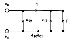
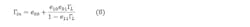
This is an equation with three unknowns, as we don’t need to know e10 and e01 separately. We need only apply three known ΓL loads and measure three Γin values to find them. The three ΓL values may be Open, Short, and Load, or +1, −1, and 0, if we had perfect calibration standards. Note that if a perfect Load is applied, the fraction will be zero and the input reflection coefficient will be simply e00, the directivity error. This is an important result, because it highlights the significance of this error in the total 1-port measurement error.
There’s a very convenient matrix operation to find e00, e10e01, and e11. Form two matrices C and V:2
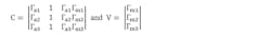
where Γa1, Γa2, and Γa3 are the three actual load values, which must be known. These are usually the Open, Short, and Load calibration standards. Γm1, Γm2, and Γm3 are the three measured input reflection coefficients with the three known loads applied.
Note that the three applied loads might also be three total reflections with different delays, whereby they’re widely separated on the Smith Chart, such as 0°, 120°, and 240°. Any three calibration standards may be used if they remain far apart on the Smith Chart over the frequencies of calibration. Open, Short, and Load are the simplest because the Open and Short will maintain a 180° difference on the circumference if they have equal internal delays, and the 50-Ω load is at (or near) the center.
Next, we calculate matrix E:
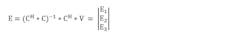
where H is the Hermitian transpose operator, or the matrix transposed with its entries conjugated.
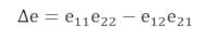
From E, we can find the three error terms:

Note that (CH * C)−1 * CH is a least-squares calculation. If our measurements are a little noisy, we can improve our results by making more known measurements and add more rows to C and V. Matrix E will still have three values in the end, and the results will be somewhat better in the face of slightly noisy measurements.
The last three error terms can be found now that the error terms on the left-hand side are known. e22 and e10e32 are found mathematically and e30, the isolation, is found by a last measurement with no connection between the two ports.
We’ll find e10e32 and e22 on the right-hand side of the forward model. First, the test cables are terminated, and measuring S21 gives isolation term e30 directly. Then with the two ports—or test cables—connected directly together:

where:
and:

This process is repeated in the reverse direction to obtain the six primed error terms of the reverse model. With all 12 error terms, we can now convert measured S-parameters into actual S-parameters of the DUT. The equations for this are given in Reference 4.
The assumption that the two cables are connected directly together greatly simplified these last two calculations. If using a Thru with some loss and delay instead, it’s easier to revert to the 8-term error model and use the “unknown Thru” or SOLR calibration calculation.5 This method doesn’t require precise knowledge of either the loss or the delay of the Thru calibration standard.
Conclusion
We’ve seen here how the measurement system can be modeled as a perfect VNA with error boxes on either side and how those errors can be related to real-world phenomena. We provided an example of the 1-port calibration calculation and then the final calculations to achieve a 2-port calibration.
With these error terms characterized, do we now have a perfect measurement? No, we will still have residual errors. These residual errors may be traced back to several factors, not the least of which are the uncertainties of the calibration kit standards. This will be a topic for the next article in the series.
Acknowledgments
The great majority of the work on VNA calibration was done by Douglas Rytting,3 and this paper draws extensively from his published work. The intention of this article is to elaborate on that work and make it more accessible to those without extensive VNA experience.
Read more articles in the TechXchange: Vector Network Analyzers.
References
1. Mason, Samuel, “Feedback Theory – Further Properties of Signal Flow Graphs”, Proceedings of the IRE (Volume: 44, Issue: 7, July 1956).
2. Walker, Brian, “One-Port VNA Calibration: A Look Under the Hood,” Microwaves & RF, Jan 11, 2021.
3. Rytting, Douglas, “Network Analyzer Error Models and Calibration Methods,” University of Illinois, Urbana-Champaign.
4. Walker, Brian, “Introduction to the Metrology of VNA Measurement,” Appendix A, May 31, 2022.
5. Walker, Brian, “VNA Master Class: Full 2-Port VNA Calibration Math Explained,” Webinar.
About the Author
Brian Walker
Senior RF Engineer SME, Copper Mountain Technologies
Brian Walker is the Senior RF Engineer SME at Copper Mountain Technologies where he helps customers to resolve technical issues and works to develop new solutions for applications of VNAs in test and measurement.
Previously, he was the Manager of RF design at Bird Electronics, where he managed a team of RF Designers and designed new and innovative products. Prior to that he worked for Motorola Component Products Group and was responsible for the design of ceramic comb-line filters for communications devices. Brian graduated from the University of New Mexico, has 40 years of RF Design experience, and has authored three U.S. patents.
