Using a VNA Like a Time-Domain Reflectometer
Members can download this article in PDF format.
What you’ll learn:
- The basic concepts underpinning time-domain reflectometry.
- Difference between frequency- and time-domain analysis.
- Some applications of TDR measurements.
Time-domain reflectometry (TDR) is a technique that measures and displays the impedance of a network (cable, filter, and so on) over time. Traditionally, this is done with a device that generates very fast pulses, injects them on the network, and measures the time and amplitude of reflected pulses.
TDR yields information about the impedance as a function of the time it takes for a pulse to reflect or travel through the medium. And, because the signals travel with (nearly) the speed of light, the time can be translated to a distance through a cable or network.
The same kind of measurement can be taken using a vector network analyzer (VNA), but in a roundabout way. A VNA measures the (reflected) impedance over frequency. We can use a Fourier transform to convert this into a series of impedances over time, just as that produced by a TDR instrument.
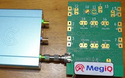
This article describes frequency and TDR measurements of coax networks and the analysis of PCB trace impedances on a test PCB, which are some of the applications of TDR analysis. The measurements were done with a MegiQ VNA-0460e 6-GHz vector network analyzer.
A Simple TDR Measurement
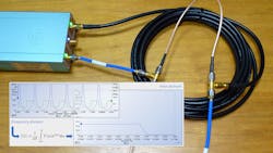
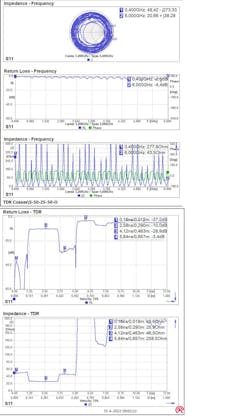
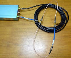
The following graphs show a measurement of a piece of 50-Ω coax terminated with a short. Figure 1 shows the setup of this measurement.
The graphs in Figure 2 are all different representations of the same S11 measurement on this network.
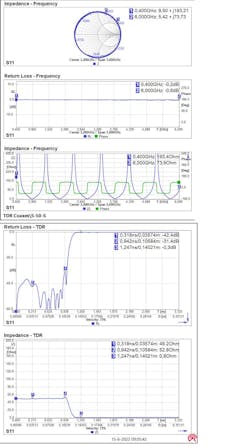
At the top of Figure 2 are three graphs of the impedance over frequency:
- In the Smith chart, the impedance is running circles around the perimeter. It’s an open impedance with increasing phase over frequency.
- The return loss is almost 0 dB because all energy is reflected by the short at the end.
- In the impedance graph, the impedance varies wildly because the signal reflected by the short termination adds or subtracts at different frequencies.
It’s difficult to discern very much about the geometry of the network from those frequency graphs.
On the bottom of Figure 2 are two TDR graphs that show the return loss and impedance over time:
- The return-loss TDR graph at the top illustrates the return loss at different times.
- The impedance graph below that shows how the impedance itself develops over time.
At T = 0, the signal leaves the VNA port. At T = 1 ns (marker 2), the signal that’s reflected by the short returns to the VNA port. The signal first travels through the 50-Ω cable and the impedance then drops to (almost) zero at the short. In a coax cable, time is distance given that the signal travels at nearly the speed of light.
The second horizontal axis (at the bottom) of the TDR graphs converts the time to the distance in the cable. The signal travels through the cable with the speed of light, multiplied by a “velocity factor” that depends on the type of cable. This velocity factor is normally on the order of 60% to 90% of the speed of light; this setting can be changed for the cable in use.
For return measurements, the distance scale accounts for the round trip of the signal from port to end and back to the port again. So, the distance scale is the actual distance from the port to the impedance drop. Of course, the VNA can’t look beyond the end of the cable. Generally, though, the graph slopes to the termination impedance.
The TDR transformation shows the real impedance at different positions in the network. A TDR signal doesn’t have phase information. This resembles the characteristic impedance of a coax cable, which also is a real number. For this reason, there’s no Smith-chart representation of a TDR signal.
Multiple Impedance Jumps
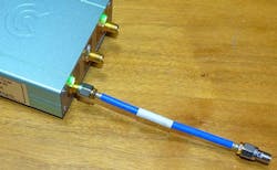
With some coax creativity, we can make a more interesting network (Fig. 3). The signal travels through a length of 50-Ω cable, then through two parallel 50-Ω cables (forming a 25-Ω line) and back again to a single cable, “terminated” with an open.
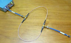
Figure 4 shows the measurements of this network. Again, the frequency graphs look spectacular, but they don’t tell us much about the structure of the network. In the TDR graphs on the bottom, the impedances and jumps are clearly visible. It transitions from 50 Ω to the 25 Ω of the two parallel cables, back to 50 Ω, and then to a high impedance at the end.
Two-Port Measurements on a Long Cable
Next, let’s connect a long 50-Ω coax to the jumping network from above and do a two-port measurement. The jumping network is made even more interesting with an additional length of coax in one arm of the split network (Fig. 5). There are now two unequal signal paths. The “far end” of the network is connected to Port 2 of the VNA; therefore, it’s terminated with 50 Ω. For Port 2, this is the “near end.”
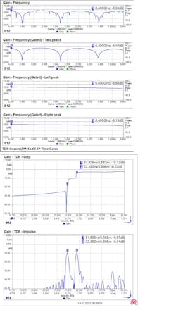
The measurement of this network is shown in Figure 6. On the top are the frequency graphs and on the bottom are the TDR graphs. The S11 Smith chart in the top portion of the figure looks like before. The S22 Smith chart seems to have a better impedance because the mismatch is located at the end of the long coax, which attenuates the reflections. The gains (S12 and S21) also vary wildly due to all of the impedance jumps in the network. Note that the forward and reverse gain (loss) are identical, as there’s no directivity in the network.
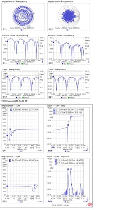
In the TDR graphs of the impedances S11 and S22, we see that the jumps are near Port 1 and far from Port 2. The addition of an extra delay in one arm of the split part gives short extra jumps in the TDR impedance (marker 1).
The TDR graphs of the gain show that the signal arrives at the other port after the delay of the network. The “Gain-TDR-Step” graph reveals that the signal arrives in two steps. This two-step arrival is clearer with the impulse mode of the TDR transform. There are clearly two peaks in the arrival of the signal at the other end. The dual peaks are caused by the uneven length of the two arms of the split network part.
Distance-to-Fault Detection
As shown by the previous examples, the impedance over a length of cable is clearly visible. This is the basis for distance-to-fault (DTF) detection, which aids in locating damage in a (long) coax cable.
In the TDR graph, it’s easy to see if there are impedance jumps, like a short or open in the cable, and how far they are from the VNA. When a coax has minor damage (crushed or bent), it can show a slight or large impedance variation along its length. The advantage of TDR for fault detection is that the cable needn’t be terminated with a specific impedance, so it can be applied on long cables with no immediate control of the end point.
Time Gating
With the TDR functionality, it’s possible to “filter” the gain-frequency graph with a filter in time. Effectively, the VNA software can do a TDR transformation of the frequency measurement, remove signal components outside (or inside) a certain time range, and then transform the signal back to a frequency graph. This is known as time gating.
Figure 7 shows the definition of such a time gate on the TDR-transformed signal. Markers 1 and 2 define a time range and the filter is shown in black.
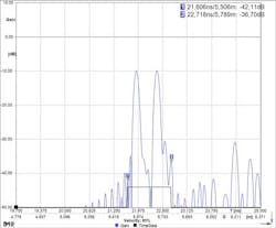
Figure 8 depicts the result of several time gates. At the top is the original gain graph, and below that is the gain with a time gate around both peaks. It shows the gain with the spurious (reflection) peaks removed. Third from top shows the gain with a time gate around the first peak, while the fourth graph is the gain with a time gate around the second peak.
Analyzing PCB Traces
TDR measurements also can be used to analyze the impedances of PCB traces and connector launch footprints. To measure these small features, the VNA has an enhanced TDR mode that uses oversampling and extrapolation of the measurement data.
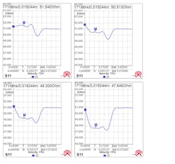
We designed a PCB with different coplanar-waveguide-with-ground (CPWG) traces and SMA-connector launches to investigate the impedances of these geometries. The PCB (Fig. 9) is a four-layer PCB with a top and bottom core of 254-µm Isola I-Tera material.
Circuits 2, 3, 6, and 7 are traces with different widths and a ground clearance of 200 µm. They’re terminated with 50 Ω (2 × 100 Ω) near the center of the PCB. The SMA connector is a solderless type that we moved to different positions. The connector was de-embedded from the measurements to view only the impedances of the traces.
The graphs in Figure 10 show the impedance of traces with widths of 430, 450, 470, and 500 µm, respectively. The impedance decreases with wider track widths. The track of 450 µm shows the best 50-Ω match. The impedance dip at the end of the trace is due to the layout of the termination network with a wider footprint that accommodates two resistors.
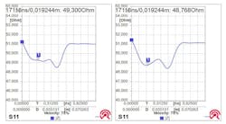
The Effect of Vias
We intended Circuit 4 (with the connector) for investigating the effect of vias. It has a trace width of 470 µm with two vias to jump to the bottom layer and back up again. The graphs in Figure 11 show the impedance of the normal 470-µm trace (left) next to the impedance of the same trace with two vias. The impedance is very similar to the regular, with a slight drop because of the vias. This suggests that the vias have an impedance like that of the 470-µm trace.
Conclusions
Where regular VNA graphs of network measurements can be confusing or complicated, TDR analysis of these measurements can provide better insight into the physical geometry of a network. Time-domain reflectometry also is useful to get better insight into local impedance effects of networks. Furthermore, time gating can be utilized to isolate certain areas in a network for frequency representation.
About the Author
Roger Denker
Managing Director, MegiQ
Roger Denker has been active in RF and wireless development for over 20 years. As an RF design consultant, he has assisted many companies in their transformation to wireless products that are sold worldwide. As managing director of MegiQ, he oversees development, production, and promotion of the company’s RF development tools.
