Finwave’s 3D GaN FinFET Technology Stands Poised to Break the mmWave PA Bottleneck
This article is part of our IMS2022 coverage.
The inroads being made by gallium nitride (GaN) technology into the 5G world are good news for everyone concerned. However, an important aspect to making mmWave 5G available and accessible to all is the development of high-power, high-linearity mmWave power amplifiers. Started in 2012 by MIT researchers as Cambridge Electronics, the company now known as Finwave Semiconductor has taken up the challenge of increasing the efficiency of mmWave power amplifiers.
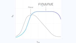
Today’s approaches to such amplifiers are throttling 5G due to their inability to deliver the higher linearity and efficiency needed to solve uplink issues facing mmWave frequencies, which do not propagate nearly as far as microwave signals. Seeing an opportunity to catalyze change, Finwave is now emerging from stealth mode to unveil its next-generation 3D gallium-nitride (GaN) technology.
With 10 times higher breakdown electric field than silicon, high electron mobility, and the ability to operate at higher junction temperature, GaN semiconductors are poised to play a significant role for the next decade's technology revolutions. At mmWave frequencies, GaN-on-silicon amplifiers excel versus alternative solutions such as Si CMOS, GaAs pHEMTs, or SiGe devices.
Finwave co-founders Prof. Tomas Palacios and Dr. Bin Lu first teamed at MIT to invent several of the foundational technologies for Finwave, including a novel type of GaN transistor based on a FinFET architecture. After being spun out of MIT, the company spent several years developing the technology further for manufacturing in the standard silicon CMOS fabs. By 2020, Finwave demonstrated the first GaN FinFETs fabricated with 8” silicon CMOS tools.
Finwave’s 3DGaN technology is said to significantly improve linearity, output power, and efficiency in 5G mmWave systems while reducing costs for carriers. By leveraging high volume 8” Si CMOS, Finwave’s devices benefit from both the cost model and scalability of silicon technology. “The combination of the outstanding electrostatic control and linearity of the GaN FinFET structure, with the cost model of silicon, and the scaling ability of state-of-the-art 8” and, in the future, 12” fabs makes 3DGaN a true game changer,” commented Palacios.
Finwave will be at the International Microwave Symposium in Denver for meetings with partners, industry experts, and other interested parties. Please contact [email protected] to schedule an informational briefing.
For more information, visit the company website.
For more IMS2022 coverage, visit our digital magazine.
About the Author

David Maliniak
Executive Editor, Microwaves & RF
I am Executive Editor of Microwaves & RF, an all-digital publication that broadly covers all aspects of wireless communications. More particularly, we're keeping a close eye on technologies in the consumer-oriented 5G, 6G, IoT, M2M, and V2X markets, in which much of the wireless market's growth will occur in this decade and beyond. I work with a great team of editors to provide engineers, developers, and technical managers with interesting and useful articles and videos on a regular basis. Check out our free newsletters to see the latest content.
You can send press releases for new products for possible coverage on the website. I am also interested in receiving contributed articles for publishing on our website. Use our contributor's packet, in which you'll find an article template and lots more useful information on how to properly prepare content for us, and send to me along with a signed release form.
About me:
In his long career in the B2B electronics-industry media, David Maliniak has held editorial roles as both generalist and specialist. As Components Editor and, later, as Editor in Chief of EE Product News, David gained breadth of experience in covering the industry at large. In serving as EDA/Test and Measurement Technology Editor at Electronic Design, he developed deep insight into those complex areas of technology. Most recently, David worked in technical marketing communications at Teledyne LeCroy, leaving to rejoin the EOEM B2B publishing world in January 2020. David earned a B.A. in journalism at New York University.
