Capitalize on EDA When Developing MIMO, Phased-Array Antenna Systems, Part 2
Download this article as a.PDF
Part 1 of this two-part series discussed the development costs and complexity of new radar and communications systems utilizing phased-array antennas, and how these challenges are being addressed through new functionalities in electronic-design-automation (EDA) software. Part 2 delves into individual antenna-element development and its incorporation into an array simulation that accounts for mutual coupling between radiating elements, as well as positioning (edge, center, corner) within the array and impairments due to element failure.
Individual Antenna Design
From the example in Part 1, a 15-×-5 array presented the radiation patterns for an ideal isotropic antenna (gain = 0 dBi) and a simple patch antenna. In addition to the array configuration itself, the design team will likely want to specify the radiation pattern and size constraints for the individual antenna elements. This operation can be performed using the synthesis capabilities in the AntSyn antenna synthesis and optimization module within NI AWR Design Environment.
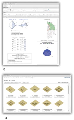
AntSyn uses an electromagnetic (EM) solver driven by proprietary evolutionary algorithms to explore multiple design options based on antenna specifications defined by the engineer. These specifications include typical antenna metrics, physical size constraints, and optional candidate antenna types (the user may select from a database of antenna types or let the software automatically select likely antenna types to optimize; Fig. 1).
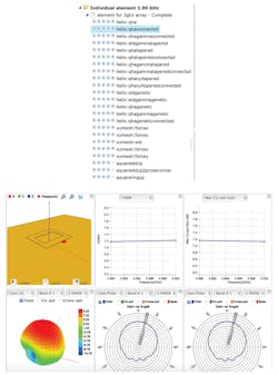
AntSyn creates antenna geometries from its database of design types. It then applies EM simulation and its unique evolutionary optimization to modify those designs to achieve the required electrical performance and size constraints. A run-time update of the design types under investigation is listed, along with a star rating system to indicate which designs are close to achieving the desired performance.
Users are able to review the results and design styles as the simulation progresses. Promising designs can then be exported into an AWR Design Environment EM tool (AXIEM 3D planar simulator or Analyst 3D finite-element method simulator) or through AWR Connected third-party EM simulators (Fig. 2).
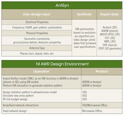
Figure 3 shows the design flow between AntSyn and NI AWR Design Environment. AntSyn takes antenna requirements and generates an antenna for use in EM tools, which will create the antenna pattern for the Visual System Simulator (VSS) phased-array model.
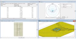
Due to its relatively small size and easy fabrication, a square-ring patch antenna was chosen from the potential antennas created by AntSyn. The antenna was exported using the AXIEM options and then imported into a new AXIEM EM structure in the initial phased-array project. Figure 4 shows the re-simulated antenna.
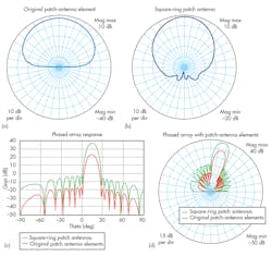
This simulation provided the antenna pattern used to replace the original patch antenna employed in the 15-×-5 phased array (Fig. 5a). The new antenna pattern is depicted in Figure 5b. The new phased-array results for both the original antenna (red trace) and the square-ring patch (green trace) can be seen in Figures 5c and 5d.
Modeling Complex Interactions
The mutual coupling between antenna elements affects antenna parameters like terminal impedances and reflection coefficients, and hence the antenna-array performance in terms of radiation characteristics, output signal-to-interference noise ratio (SINR), and radar cross section (RCS). The most recent V13 release of VSS includes new capabilities for more accurate simulation of these parameters, including enhanced modeling of element patterns and mutual coupling. What we’ll examine next are these recent advances in advanced phased-array modeling, including accurate representation of the feed structure.
As mentioned, VSS lets designers define gains or full radiation patterns for each antenna element in the phased array. Thus, they can use different radiation patterns for internal, edge, and corner elements of the phased array (Fig. 6).
The radiation pattern of each antenna element will likely be affected by its position in the phased array. These patterns may be measured in the lab or calculated in AXIEM or Analyst. A simple approach to characterize the appropriate radiation pattern for a given element is to use a 3-×-3 phased array. One element is then excited, while all others are terminated. This one excited element could either be the internal element, one of the edge elements, or one of the corner elements.
The method described will provide the internal, edge, and corner element radiation patterns, which can then be automatically stored in data files using the NI AWR software output data file measurements (the same technique used in the example above). This approach includes the effect of mutual coupling from first-order neighbors. An array with a larger number of elements may be used to extend mutual coupling to first- and second-order neighbors.
It is also important to capture the mutual coupling between neighboring elements. The VSS phased-array model does this through a coupling table defined in the configuration file. Different coupling levels can be defined based on distance from each other. In Figure 7, the coupling, which is specified in magnitude (dB) and phase (degrees), is defined for two different distances (adjacent side elements: radius c_1 and adjacent corner elements: radius c_2).
Modeling Impairments and Yield Analysis
RF hardware impairments of the array will affect the resulting side-lobe levels and beam patterns and ultimately reduce system-level performance. For transmitter arrays, side-lobe levels from imperfectly formed beams may interfere with external devices or make the transmitter visible to countermeasures. In radar systems, side lobes may also cause a form of self-induced multipath, where multiple copies of the same radar signal arrive from different side-lobe directions, which can exaggerate ground clutter and require expensive signal processing to remove. Therefore, it is critical to identify the source of such impairments, observe their impact on the array performance, and take steps to reduce or eliminate them.
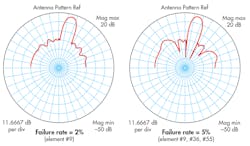
The VSS phased-array configuration file allows engineers to simulate array imperfections due to manufacturing flaws or element failure. All gain/phase calculations are performed internally and yield analysis can be applied to the block to evaluate sensitivity to variances of any defining phased-array parameters. As an example, VSS was used to perform an element failure analysis on a 64-element (16-×-4) array, producing the plots in Figure 8, which illustrates the side-lobe response degradation.
RF impairments can also be caused by any number of items relating to the feed network design and related components. Systematic errors that may be compensated include inter-chain variations caused by asymmetrical routing (layout); frequency dependencies; noise; temperature; and varied mismatching due to changing antenna impedance with steer angle, which also impacts amplifier compression. Therefore, it is imperative to be able to simulate the interactions between the antenna array and the individual RF links in the feed network.
RF Link Modeling
NI AWR software products include the simulation and modeling technology to capture these impairments accurately and incorporate results into the VSS phased-array assembly model. This is an important functionality, since RF links are not ideal and can cause the array behavior to deviate significantly. The phased-array assembly can operate in either the RX or TX mode, supporting the configuration of the array-element geometry, each element's antenna characteristics, the RF link characteristics, and the common linear characteristics of the combiner/splitter used to join the elements together.
The configuration is performed primarily through a text data file. Commonly swept settings are specified either directly via block parameters (such as steering angles), or specified in the data file but capable of being overridden via block parameters (such as individual element gain and phase adjustments).
The configuration of the phased-array assembly may be divided into several sections:
- Array geometry: Defines the number of elements, their placement, and any geometry-related gain and phase tapers.
- Antenna characteristics: Defines antenna gain, internal loss, polarization loss, mismatch loss, and radiation patterns for both receive and transmit configurations.
- RF-link characteristics: Defines links for individual elements, including gain, noise, and 1-dB compression point (P1dB). Supports two-port RF nonlinear amplifiers using large-signal nonlinear characterization data typically consisting of rows of input power or voltage levels and corresponding output fundamental, harmonic, and/or intermodulation product levels. Frequency-dependent data is also supported.
- Assignment of antenna and RF-link characteristics to individual elements.
- Power splitter characteristics: Splits the incoming signal into n-connected output ports.
- Mutual coupling characteristics (previously discussed).
One common challenge is that not all RF links should be equal. For example, gain tapers are commonly employed in phased arrays. However, when identical RF links are used for all antenna elements, elements with higher gains may operate well into compression while others operate in a purely linear region, causing undesired array performance. To avoid this problem, designers often use different RF-link designs for different elements. While this is a more complicated task, the designs can be achieved with VSS phased-array modeling, resulting in more efficient phased arrays.
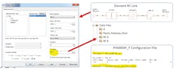
To assist the design team creating the feed network and providing the RF link to the systems team, VSS includes the capability to automatically generate the characteristics of the phased-array element link defined by the data tables. The designer starts by creating a schematic-based link design per the system requirements. A “measurement” extracts the design characteristics (including circuit-level design details like nonlinearities) through NI AWR Design Environment Microwave Office co-simulation, and saves a properly formatted data file for use with the phased-array assembly model (Fig. 9).
In-Situ Nonlinear Simulations
An accurate simulation must also account for the interactions that occur between the antenna elements and the driving feed network. The problem for simulation software is that the antenna and the driving feed network influence each other. The antenna’s pattern is changed by setting the input power and relative phasing at its various ports. At the same time, the input impedances at the ports change with the antenna pattern. Since input impedance affects the performance of the nonlinear driving circuit, the changing antenna pattern impacts overall system performance.
In this case, the input impedance of each element in the array must be characterized for all beamsteering positions. The array is only simulated once in the EM simulator. The resulting S-parameters are then used by the circuit simulator, which also includes the feed network and amplifiers. As the phase shifters are tuned over their values, the antenna’s beam is steered. At the same time, each amplifier sees the changing impedance at the antenna input to which it is attached. Thus, the amplifier’s performance is affected.
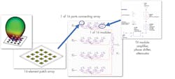
In this final example, the power amplifiers (PAs) are nonlinear, designed to operate at their P1dB for maximum efficiency. They are, therefore, sensitive to the changing load impedances presented by the array. The beam of a 16-element array is steered by controlling the relative phasing and attenuation to the various transmit modules (Fig. 10). In practice, the harmonic balance simulation in Microwave Office used to characterize the PAs takes substantial time to run with 16 PAs. Therefore, the beam is steered with the amplifiers turned off. The designer then turns on the individual PA for specific points of interest after obtaining the load impedance from the directed antenna.
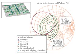
At this point, the designer can directly investigate the PA’s nonlinear behavior as a function of the load (antenna) impedance. With the load-pull capability in Microwave Office, PA designers can investigate output power, compression, and any other number of nonlinear metrics defining the amplifier’s behavior (Fig. 11).
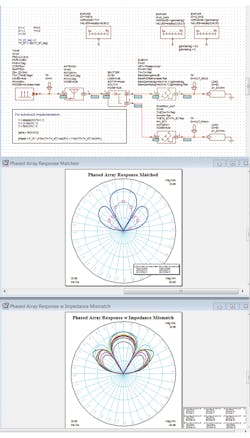
With a detailed characterization of the RF links for each individual element, the overall system simulation is able to indicate trouble areas (Fig. 12). These issues would have previously gone undetected until expensive prototypes were made and tested in the lab.
Conclusion
The capability to design and verify the performance of the individual components, along with the entire signal channel that defines the AESA radar, is a necessity due to increasing element counts and advances in antenna/electronics integration. Through a sophisticated design flow that encompasses circuit simulation, system-level behavioral modeling, and EM analysis operating within a single design platform, development teams can investigate system performance and component-to-component interaction prior to costly prototyping.
About the Author
David Vye
Technical Marketing Director, Cadence
David Vye is the senior product marketing manager for AWR software at Cadence, where he’s responsible for product messaging and positioning in the RF/microwave market. A former editor and business development manager for Microwave Journal, David has held a number of technical and marketing positions throughout the RF/microwave industry. He holds a BSEE from the University of Massachusetts at Dartmouth, with a concentration in microwave engineering.
