New Development in Semiconducting Film for 2D Electronic Components
Advancements have been made in the controlled growth of uniform atomic layers of molybdenum disulfide (MDS). This semiconductor compound is one of the necessary materials for creating functioning, 2D electronic components with atom-thick circuits.
Scientists at Rice University and Oak Ridge National Laboratory (ORNL) worked to see if large, high-quality, atomically thin MDS sheets could be grown in a chemical-vapor-deposition (CVD) furnace to be analyzed. They hope that MDS could be joined with graphene (which has no band gap) and hexagonal boron nitride (hBN) (an insulator) to form field-effect transistors, integrated logic circuits, photodetectors, and flexible optoelectronics.
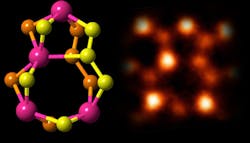
MDS is distinct from the other necessary materials because it doesn’t lay flat. When viewed from above, it is actually a stack with a layer of molybdenum atoms between two layers of sulfur atoms. Scientists see many potential ways for combing the materials in both two-dimensional and three-dimensional stacks and varying compositions.
Previous methods of growing MDS proved difficult, with the results too small for use. Researchers have discovered, however, that adding artificial edges allows the material to properly nucleate, with grain sizes growing up to 100 µm.
The abstract can be read here.
About the Author
Iliza Sokol
Associate Digital Editor
Iliza joined the Penton Media group in 2013 after graduating from the Fashion Institute of Technology with a BS in Advertising and Marketing Communications. Prior to joining the staff, she worked at NYLON Magazine and a ghostwriting firm based in New York.

