L-Band GaN-on-SiC RF PA Module Delivers 29-dB Gain, 100-W Output
This article appeared in Electronic Design and has been published here with permission.
Despite all of the justified attention given to the part of gigahertz spectrum ranging from upper single-digit, lower double-digit, and even higher frequencies, there’s still lots of important activity at the very lowest end of that gigahertz world. And that means that RF components such as power amplifiers are still important.
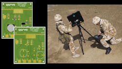
Addressing this need, Qorvo Inc. introduced its QPA2511 GaN-on-SiC power-amplifier module (PAM) targeting commercial and defense radar applications (Fig. 1).
Qorvo maintains this is highest-gain, 100-W output L-band compact solution available. The two-stage amplifier operates at pulsed RF CW in frequency range of 1.2 to 1.4 GHz, typically providing 50 dBm of saturated output power with 29 dB of large-signal gain. It operates from a 50-V supply and offers 60% power added efficiency (PAE) with a resultant circuit size that’s claimed to be 70% smaller than equivalent two-stage solutions.
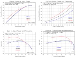
The 13-page datasheet contains the necessary graphs and tables, including the four figures that RF designers often use for their “first-pass” assessment (Fig. 2).
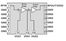
The QPA2511 is matched to 50 Ω with integrated bias circuits and a dc-blocking capacitor at its input port. The robust, rectangular, 48-pin surface-mount package measures just 25 × 12.5 × 3.5 mm, thus simplifying system design, board assembly, and testing (don’t worry, most of those 48 pins are devoted to RF and power grounds). Operating temperature range is −40 to +85°C.
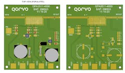
The datasheet also shows a basic evaluation board, approximately 75 × 90 mm, using Rogers 4350B PCB material, along with its schematic and bill of materials consisting of the RF PA; an array of bypass capacitors and two bulk-filtering capacitors; test points and jumpers; a ferrite bead; and two SMA connectors. In addition, there’s an image of the board, both populated and bare (Fig. 3). It’s also available on request as the QPA2511EVBPLPR2 evaluation board.
About the Author

Bill Schweber
Contributing Editor
Bill Schweber is an electronics engineer who has written three textbooks on electronic communications systems, as well as hundreds of technical articles, opinion columns, and product features. In past roles, he worked as a technical website manager for multiple topic-specific sites for EE Times, as well as both the Executive Editor and Analog Editor at EDN.
At Analog Devices Inc., Bill was in marketing communications (public relations). As a result, he has been on both sides of the technical PR function, presenting company products, stories, and messages to the media and also as the recipient of these.
Prior to the MarCom role at Analog, Bill was associate editor of their respected technical journal and worked in their product marketing and applications engineering groups. Before those roles, he was at Instron Corp., doing hands-on analog- and power-circuit design and systems integration for materials-testing machine controls.
Bill has an MSEE (Univ. of Mass) and BSEE (Columbia Univ.), is a Registered Professional Engineer, and holds an Advanced Class amateur radio license. He has also planned, written, and presented online courses on a variety of engineering topics, including MOSFET basics, ADC selection, and driving LEDs.


