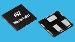
Si Driver/GaN Power-Transistor Combo Promises Smaller, Faster Chargers and Power Supplies
Combining a silicon-based half-bridge driver and a pair of gallium arsenide (GaN) transistors, STMicroelectronics’ new MasterGaN family of devices is expected to form the foundation of next-generation compact and efficient chargers and power adapters for applications up to 400 W. That means smaller, ultra-fast smartphone chargers, wireless chargers, USB-PD adapters for PCs and gaming, and industrial applications such as solar-energy storage systems, uninterruptible power supplies, and OLED TVs.
Today’s GaN market is typically served by discrete power transistors and driver ICs, which designers must integrate for optimal performance. In what’s called a first, ST’s MasterGaN approach saves that time and effort while also assuring a high level of performance. Other benefits include a smaller footprint, simpler assembly, and higher reliability. Chargers and adapters based on MasterGaN can cut 80% of the size and 70% of the weight of all-silicon-based implementations.
The MasterGaN platform leverages STDRIVE 600-V gate drivers and GaN high-electron-mobility transistors (HEMTs). The 9-mm x 9-mm, 1-mm-profile GQFN package ensures high power density and is designed for high-voltage applications with over 2-mm creepage distance between high-voltage and low-voltage pads.
The family of devices will span different GaN-transistor sizes (RDS(ON)) and will be offered as pin-compatible half-bridge products that let engineers scale successful designs with minimal hardware changes. Leveraging the low turn-on losses and absence of body-diode recovery that characterize GaN transistors, the products enhance the performance of high-end, high-efficiency topologies such as flyback or forward with active clamp, resonant, bridgeless totem-pole PFC (power factor corrector) and other soft- and hard-switching topologies used in AC/DC and DC/DC converters and DC/AC inverters.
The initial member of the device family is MasterGaN1, which is connected as a half bridge with integrated high-side and low-side drivers. The MasterGaN1 contains two normally-off transistors that feature closely matched timing parameters, 10-A maximum current rating, and 150-mΩ on-resistance (RDS(ON)). The logic inputs are compatible with signals from 3.3 V to 15 V. Comprehensive protection features are also built in, including low-side and high-side UVLO protection, interlocking, a dedicated shutdown pin, and over-temperature protection.
MasterGaN1 is in production now and is priced at $7 in quantities of 1,000. An evaluation board is also available.
STMicroelectronics, www.st.com.
About the Author
David Maliniak
Executive Editor, Microwaves & RF
I am Executive Editor of Microwaves & RF, an all-digital publication that broadly covers all aspects of wireless communications. More particularly, we're keeping a close eye on technologies in the consumer-oriented 5G, 6G, IoT, M2M, and V2X markets, in which much of the wireless market's growth will occur in this decade and beyond. I work with a great team of editors to provide engineers, developers, and technical managers with interesting and useful articles and videos on a regular basis. Check out our free newsletters to see the latest content.
You can send press releases for new products for possible coverage on the website. I am also interested in receiving contributed articles for publishing on our website. Use our contributor's packet, in which you'll find an article template and lots more useful information on how to properly prepare content for us, and send to me along with a signed release form.
About me:
In his long career in the B2B electronics-industry media, David Maliniak has held editorial roles as both generalist and specialist. As Components Editor and, later, as Editor in Chief of EE Product News, David gained breadth of experience in covering the industry at large. In serving as EDA/Test and Measurement Technology Editor at Electronic Design, he developed deep insight into those complex areas of technology. Most recently, David worked in technical marketing communications at Teledyne LeCroy, leaving to rejoin the EOEM B2B publishing world in January 2020. David earned a B.A. in journalism at New York University.


