DSP Architecture Targets 5G Endpoints and Radio Access Networks
CEVA’s new Gen4 CEVA-XC DSP architecture unifies the principles of scalar and vector processing in a powerful architecture, enabling two-times 8-way VLIW and up to 14,000 bits of data-level parallelism. It incorporates an advanced, deep pipeline architecture enabling operating speeds of 1.8 GHz at a 7nm process node using a unique physical design architecture for a fully synthesizable design flow, and an innovative multithreading design. This allows the processors to be dynamically reconfigured as either a wide SIMD machine or divided into smaller simultaneous SIMD threads. The Gen4 CEVA-XC architecture also features a novel memory subsystem, using 2048-bit memory bandwidth, with coherent, tightly coupled memory to support efficient simultaneous multithreading and memory access.
CEVA’s Gen4 CEVA-XC DSP architecture handles highly complex parallel processing workloads required for 5G endpoints and Radio Access Networks (RAN), enterprise access points, and other multigigabit low-latency applications.
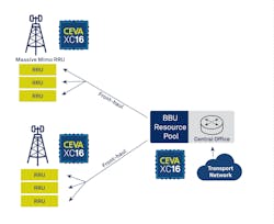
The first processor based on the Gen4 CEVA-XC architecture is the multicore CEVA-XC16, touted as the fastest DSP ever made. It is targeted for the rapid deployment of different form factors of 5G RAN architectures including Open RAN (O-RAN) and baseband-unit (BBU) aggregation as well as Wifi and 5G enterprise access points. The CEVA-XC16 is also applicable to massive signal processing and AI workloads associated with base station operation.
The CEVA-XC16 has been specifically architected with the latest 3GPP release specifications in mind, building on the company’s extensive experience partnering with leading wireless infrastructure vendors for their cellular infrastructure ASICs. The previous generation CEVA-XC4500 and CEVA-XC12 DSPs power 4G and 5G cellular networks today, and the new CEVA-XC16 is already in design with a leading wireless vendor for its next-generation 5G ASIC.
The CEVA-XC16 offers high parallelism of up to 1,600 GOPS (Giga Operations Per Second) that can be reconfigured as two separate parallel threads. These can run simultaneously, sharing their L1 data memory with cache coherency, which directly improves latency and performance efficiency for PHY control processing, without the need for an additional CPU. These new concepts boost the performance per square millimeter by 50% compared to a single-core/single-thread architecture when massive numbers of users are connected in a crowded area. This amounts to 35% die area savings for a large cluster of cores, as is typical for custom 5G base station silicon.
Other key features of the CEVA-XC16 include:
• Latest generation dual CEVA-BX scalar processor units, which enable true simultaneous multithreading
• Dynamic allocation of vector units resources to processing threads, which facilitates optimal vector unit resource utilization and reduced overhead of complex flows
• Advanced scalar control architecture and tools, with 30% code size reduction from previous generations, using latest dynamic branch prediction and loop optimizations, and an LLVM based compiler
• New instruction-set architectures for FFT and FIR, resulting in 2X performance improvement
• Enhanced multi-user capabilities supporting massive bandwidth allocation of single-user as well as fine-granularity user allocations
• Simple software migration path from earlier CEVA-XC4500 and CEVA-XC12 DSPs
The CEVA-XC16 is available for general licensing starting in Q2 2020.
About the Author
David Maliniak
Executive Editor, Microwaves & RF
I am Executive Editor of Microwaves & RF, an all-digital publication that broadly covers all aspects of wireless communications. More particularly, we're keeping a close eye on technologies in the consumer-oriented 5G, 6G, IoT, M2M, and V2X markets, in which much of the wireless market's growth will occur in this decade and beyond. I work with a great team of editors to provide engineers, developers, and technical managers with interesting and useful articles and videos on a regular basis. Check out our free newsletters to see the latest content.
You can send press releases for new products for possible coverage on the website. I am also interested in receiving contributed articles for publishing on our website. Use our contributor's packet, in which you'll find an article template and lots more useful information on how to properly prepare content for us, and send to me along with a signed release form.
About me:
In his long career in the B2B electronics-industry media, David Maliniak has held editorial roles as both generalist and specialist. As Components Editor and, later, as Editor in Chief of EE Product News, David gained breadth of experience in covering the industry at large. In serving as EDA/Test and Measurement Technology Editor at Electronic Design, he developed deep insight into those complex areas of technology. Most recently, David worked in technical marketing communications at Teledyne LeCroy, leaving to rejoin the EOEM B2B publishing world in January 2020. David earned a B.A. in journalism at New York University.


