Electronic Components Created by Printing Onto Substrates
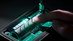
High-quality components like sensors and heating elements are being printed directly onto substrates at the binder Innovation and Technology Center (ITZ) in Bad Rappenau, Germany. The company prints electronic structures onto the surface of components, allowing for relocation of functions within an electronic system, often reducing the need for parts such as cables and connectors within the system.
The production-ready printing process also saves assembly time and effort, and it enables the execution of new functions within restricted system spaces. Substrates include plastic, metal, glass, and ceramic materials, while conductors are formed of pastes based on silver, copper, carbon, and other materials.
Dr.-Ing. Martin Ungerer, Team Leader Printed Electronics at binder ITZ, explained, “Printed electronics shifts the limit of what a single component can achieve. We apply conductor tracks, heating functions, or sensor technology directly onto the surface, saving a whole range of individual parts and creating intelligent components. At the ITZ, we develop these processes through to application maturity.”
Ungerer added that prototypes are quickly moved to production. “The binder group then turns the functional prototype into a production-ready solution. This path from idea to series production is something pure printing specialists cannot offer in this form.”
Various printing processes are researched and used at the ITZ, but the binder group network also collaborates closely with customers to implement their specific design and production needs. Its vertically integrated structure enables complete assembly of system designs, including the addition of interconnections, to provide customer-specific integrated solutions that use printed electronics (see image above).
Learn more about printing technologies
About the Author
Jack Browne
Technical Contributor
Jack Browne, Technical Contributor, has worked in technical publishing for over 30 years. He managed the content and production of three technical journals while at the American Institute of Physics, including Medical Physics and the Journal of Vacuum Science & Technology. He has been a Publisher and Editor for Penton Media, started the firm’s Wireless Symposium & Exhibition trade show in 1993, and currently serves as Technical Contributor for that company's Microwaves & RF magazine. Browne, who holds a BS in Mathematics from City College of New York and BA degrees in English and Philosophy from Fordham University, is a member of the IEEE.