Transform Connector Design and Manufacturing for 5G Connectivity

Members can download this article in PDF format.
What you’ll learn:
- Higher operating frequencies are causing components to shrink, calling for creativity in interconnects.
- Designers must deploy a comprehensive, multidisciplinary methodology to approach 5G product development as an integrated system and not merely the sum of disparate parts.
- Growing demands for multiband transmission and lower power consumption will require lower insertion losses on RF components.
The steady and relentless emergence of 5G technology is rearranging and redefining our lives. But reaping the full potential of 5G wireless technology requires careful calibration and coordination involving a host of product design, development, and manufacturing people as well as processes.
With 5G comes a steady acceleration toward higher operating frequencies to facilitate faster data rates and lower latency. While these advances are ushering in a new era of communications and connectivity, they need to be calibrated and coordinated with the constant drive for increasingly smaller and more powerful devices. These include the latest smartphones, tablets, smartwatches, wearables, medical devices, drones, and much more.
Designers of 5G-enabled devices are faced with a multitude of product development obstacles, performance considerations, and complex connectivity challenges. However, collaborative problem-solving helps minimize major product design and manufacturing roadblocks. More holistic development methodologies can reduce the barrage of challenges by taking advantage of cross-disciplinary skills in antenna, signal integrity, battery, thermal, and alternative-packaging solutions.
Addressing the Challenges
It takes a delicate balance between electrical, mechanical, and power-management requirements to clear many 5G hurdles, including demands for greater antenna density, increased battery power, and more features. An additional layer of complexity involves supporting increasing numbers of smaller components, including connectors, so that everything can fit on a printed circuit board (PCB) roughly the size of a grain of rice.
At the same time, there’s an increased need for connector consolidation, in line with the theme of “do more with less,” which resonates throughout the entire process. In addition, ensuring 5G-enabled components meet heightened ruggedization thresholds requires product developers to take a closer look at components and materials, as what they used in 4G products may not be compatible with, or meet the durability needs of, next-generation infrastructure and gear.
Miniaturization experts question whether the trajectory of Moore’s Law can be maintained—the laws of physics are approaching their limits amid escalating costs of further component shrinkage. In the short term, companies are taking advantage of specialty chips to handle different functions, such as graphics processing units (GPUs), as well as artificial intelligence or video accelerators. Longer-term solutions include the use of quantum computers, graphene processing, and memristors, which can retain data without power.
Connectivity Without Fail
On average, 5G-enabled smartphones contain 15 board-to-board connectors, and the market delivers more than 1 billion units annually. While always considered essential, the role of connectors is gaining prominence for ensuring 100% reliability and seamless interconnectivity between components and boards. Whether the application requires connectors that are wire-to-wire, wire-to-board, board-to-board, flexible flat cable, flexible printed circuit, or others, they’re conduits for linking all of the disparate parts so that power and signals can reliably interact.
In the past, connectors were considered a limiting factor when it came to determining the size of a product. Thus, it’s imperative to create new ways to reduce pitch size, allowing smaller boards and higher pin densities to support the needs of broadening I/O demands. As the space inside 5G-enabled devices becomes more crowded with millimeter-wave (mmWave) antenna modules and other components, though, there’s increased pressure to reduce the size and configuration of connectors and interconnect solutions.
The answer isn’t always continually shrinking connector pins, but rather to find paths beyond traditional design limitations through creative connector layouts. For example, Molex’s Quad-Row Board-to-Board Connectors feature the industry’s first staggered-circuit layout, which achieves 30% space savings over conventional connector designs (see figure).
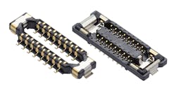
The pins are positioned across four rows at a signal contact pitch of 0.175 mm, enabling device makers to add more features, sensors, and functionality without impacting performance. Another possible tactic is to use connectors of different heights, enabling manufacturers to apply the Z-axis in optimizing component placement.
Additional antenna modules, increased RF functionality, and bigger batteries pressure product developers to shrink other components, and RF connectors often feel the pinch. In the past, coaxial cables carried RF signals from board to board, but the trend today is to use smaller RF connectors. This is driving new innovations involving miniaturization.
Other solutions, such as Molex’s Flex-to-Board RF Connector 5G25 series of compact connectors, enable designers of RF antenna modules and mobile devices to combine RF and non-RF signals. This reduces the need for additional connectors and, in turn, leads to further space and cost savings.
The reality is that 5G mmWave applications require stringent signal integrity at higher frequencies up to 40 GHz. As a result, it amps up the pressure on product designers to optimize high-speed 5G components while alleviating space constraints on increasingly crowded PCBs.
Driving Innovation in 5G Design and Manufacturing
Miniaturization isn’t just about making parts smaller—it also involves designing components that can be easily and reliably manufactured and assembled. The demand for smaller and higher performing products shows no signs of slowing.
Thus, designers and manufacturers must ask themselves just how small components can be? While the answer is arguably uncertain, one element is undeniable: The process will require embracing a new set of best practices so that designers can continue to push the technology envelope.
Designers must deploy a comprehensive, multidisciplinary methodology to approach 5G product development as an integrated system and not merely the sum of disparate antenna, PCB, packaging, connector, thermal, and other parts. Particularly in the consumer electronics space, designs need to accommodate higher RF signal frequencies and faster data transmissions. This requires product designers to optimize system designs by employing solutions to reduce RF and digital signal noise.
Therefore, it’s critical to optimize electromagnetic compatibility (EMC) throughout the entire system to support higher-frequency demands. For example, the 5G25 RF mmWave connectors feature full electromagnetic-interference (EMI) shielding, including RF terminal and full connector shielding to help ensure high signal quality. Overall signal-integrity stability is boosted by employing a ground cover-in-contact with receptacle and plug to isolate each RF signal on the connector.
Increasingly, smaller pins and contacts mean less material to make connections, which imposes stricter limits on the number of signals or amount of power possible. Today, connectors typically must perform multiple duties in devices, from carrying 5G signals or cellular and Wi-Fi communications to power and other signaling. As a result, shielding becomes more difficult and important, requiring walls between pins and external enclosures for the connectors.
Engineering for Manufacturing
Electrical considerations aren’t the only criteria calling for non-traditional thinking. Enter engineering for manufacturing. With connectors getting smaller—and more fragile—fabrication and assembly get more complex and complicated.
For example, antenna arrays are shrinking to accommodate high frequencies because their operating frequency is inversely proportional to their size. The result creates etching challenges for PCB fabrication, components, and packaging manufacturing that must be addressed from the initial design phase.
This means that mmWave antenna arrays can enable the development of smaller devices while providing designers with more area on their boards for additional components. This isn’t a forever fix, though, as antenna arrays will become even smaller.
It’s necessary to perform advanced simulations and testing along with rapid design iterations to ensure components perform as expected, even while they shrink in size and grow in functionality. Designers with access to 5G test chambers should achieve optimal signal-integrity performance at a quicker pace, resulting in finalizing design concepts in weeks, not months.
Product designers’ deep experience with EM/RF simulation tools and measurement equipment must be combined with manufacturers’ firm grasp of cutting-edge and accurate manufacturing technologies to keep pace with demands for next-gen 5G-enabled devices and products of all kinds.
Collaboration and Cooperation Counts
It’s crucial for product designers and manufacturers to join forces in devising an additive approach for fabricating components targeted at mmWave applications. First, design teams need to plan when 5G antenna arrays reach the limit of what can be fabricated due to very high-precision acceptable tolerances of antenna elements for higher frequencies. This will necessitate the exploration of process change options, such as moving from subtractive to additive manufacturing to make the required extremely fine and high-precision traces.
Other options include the ability to leverage substrate material with lower dielectric constant, as well as take advantage of novel space-saving options, such as Quad-Row, to free much needed space for specific functions impeded by manufacturing capabilities. Still, the day will come when demand exceeds the boundaries of standard and additive processing.
Advances in the design and manufacturing of critical connectors can be achieved by increasing real-time collaboration among cross-technology teams, including experts in RF, antenna, PCB, packaging, connectors, signal integrity, thermal design, and high-speed communications. Earlier cooperation among product designers also can help reduce obstacles while determining how best to pack more features and functionality into ever-smaller device form factors.
The Future of RF Connectors
Over the next three to five years, the RF connector market will continue to shift and transform to unleash new opportunities and present new obstacles for product developers. Some changes already are evident as the separation between RF designers and systems architects is narrowing to address the collective interest and scope of 5G and mmWave advances.
The ability to leverage higher frequencies for large-bandwidth utilization while ensuring compatibility to massive MIMO will be key factors in supporting higher-speed transmission. This trend, in turn, will have a major impact on RF connector and RF front-end (RFFE) designs.
For instance, growing demands for multiband transmission and lower power consumption will require lower insertion losses on RF components. Furthermore, the overarching quest for size reduction will fuel the need to achieve higher pin-to-pin isolations and greater feature density while satisfying more stringent EMC requirements.
As product designs continue to push the limits, it’s essential that all sides take action to tear down any fences between them and engage in consistent knowledge sharing. Each component and connector require an integrated approach that blends electrical, mechanical, and manufacturing engineering to ensure optimization at every step. The future of 5G connectivity depends on it.
About the Author
Kenji Kijima
Director of Mobile Products, Molex Consumer & Commercial Division
A veteran of more than 28 years in the mobile solutions market, Kenji Kijima is director of mobile products for Molex's Consumer & Commercial Division. He has held his current position since 2018, managing Molex's board-to-board connector business with major mobile OEM customers. In April 2023, Kijima was selected to manage the company's plant improvements and innovation activities worldwide.
Before joining Molex, he worked for Sony and Sony Mobile for 23 years as a product development manager for mobile and smartphones.
