Comparing Automotive Radar RF Bandpass Filter Implementations (Part 3)

Members can download this article in PDF format.
What you’ll learn:
- How planar filter technologies compare for mmWave applications.
- Specific applications of the mmWave filters in the automotive industry.
- Design procedures for mmWave planar filters.
In Part 1 of this multi-part series, we analyzed 3D electromagnetic (EM) simulations in the frequency domain of two of six implementations of a 5th-order, Chebyshev-type RF front-end bandpass filter for automotive radar applications in the mmWave band from 76 to 81 GHz. Those implementations were rectangular metallic waveguides with H-plane iris and cylindrical posts, respectively. In Part 2, we continued our analyses with microstrip and stripline implementations. Part 3 will shift to analyses of substrate-integrated waveguide implementations and wrap up with some conclusions.
SIW Bandpass Filters
Let’s take a look at substrate-integrated waveguide (SIW) implementations of the same bandpass filter we’ve examined in other implementations in Parts 1 and 2. SIW technology has been well-established as a technology1,3,4,5 over the last decade. It mimics the structure and performance of the metallic waveguide technology but with miniaturized dimensions. The miniaturization of the dimensions depends on the dielectric constant of the material in play.
In fact, SIW technology is a printed-circuit-board (PCB) technology with some advanced design rules, especially when implementing structures in the mmWave bands. In this article, we’ll examine the implementation of a SIW bandpass filter with H-plane iris and with metallic posts. The design procedure in both cases is the following:
- Design the metallic waveguide filter equivalent.
- Transfer that design to a metallic waveguide filter filled with the dielectric material that will be used during the PCB process.
- Replace the transverse walls of the metallic waveguide filter with ground vias of the proper geometry (diameter, pitch of vias).
- Implement a proper microstrip-to-SIW transition.2
The general geometry of a SIW structure and its equivalent to a metallic waveguide1 is shown in Figure 1.
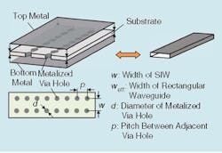
The TE10-mode related frequency region of interest is defined by:
p > d (1a)
p/λc < 0.25 (1b)
al/k0 < 10-4 (1c)
p/λc > 0.04 (1d)
where al is the total loss and k0 is the wave number in free space.
The condition (1a) states that the period length must be larger than the cylinder diameter so that the circuit is physically realizable, and (1b) is required to avoid any bandgap in the operating bandwidth of the TE10 mode and other related guided-wave modes (if involved). To be negligible, the leakage losses must respect (1c). A more restrictive and general condition for negligible leakage losses is p ≤ 2d.
Finally, a nonessential but desirable condition for the manufacturing process is for “d” to be comparable to the substrate thickness. These via cylinders are usually mechanically drilled and chemically electroplated or plasma-deposited, and the production time is directly related to the choice of a processing technique.
If the length of the period is very small with respect to the guided-wave wavelength, the mechanical rigidity is adversely affected. The number of cylinders should therefore not exceed 20 per wavelength, as stated in (1d). In the next two sections, we’ll present the 3D electromagnetic simulation results for the two SIW implementations of the bandpass filter (BPF).
SIW Bandpass Filters with H-Plane Iris
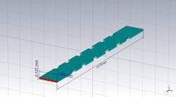
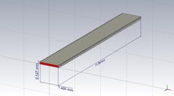
As described in the previous section, the first steps in the design procedure are to design the metallic waveguide equivalent and then transfer the design to an equivalent metallic waveguide filled with the proper dielectric. In this case, it is Rogers RO3003G2 PTFE laminate with er = 3.07. We chose a dielectric thickness of 0.127 mm. Figure 2 depicts the ideal 3D geometry.
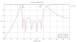
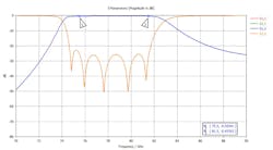
The RF performance of this filter with respect to S-parameters appears in Figure 3. The insertion loss compared to the pure metallic waveguide counterpart is increased by about 0.4 dB. The return loss is better than 22 dB. The dimensions, though, are miniaturized by a factor of 10 in the vertical dimension and by a factor of 2.5 in the horizontal dimension.
Then, according to the design procedure discussed above, the transverse walls of the waveguide are replaced by proper ground vias as shown in Figure 4. The diameter of the posts is d = 0.1 mm and the pitch is p = 0.2 mm.
To obtain those values for the via diameter, we used pitch-optimization techniques to obtain the best possible S11 in the passband and, simultaneously, the best rejection for the out-of-band areas. The RF performance of the 3D geometry of Figure 4 is shown in Figure 5.
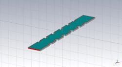
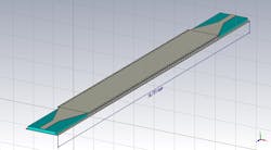
In comparing Figures 3 and 5, the insertion loss of the filter isn’t affected. However, the return loss is impacted, but it remains well above 16 dB. The main reason for the deterioration of return loss is the radiation leakage due to the limited pitch of the ground vias. The pitch is kept to a minimum of p = 0.2 mm so that one may fabricate the circuit with a normal PCB process. The final step is to implement the microstrip-to SIW-transition to finalize the design. That geometry appears in Figure 6.
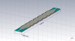
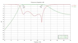
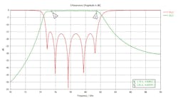
Comparing Figures 2 and 6 reveals that the additional length for each of the microstrip-to-SIW transitions is about 1.25 mm. Several types of transitions could be used,2 but the simple tapered type is most easily fabricated. The RF performance of the final geometry shown in Figure 6 is presented in Figure 7.
The insertion loss increases by 0.5 dB at mid-band compared to the non-transition case; the return loss as well as the out-of-band rejection remain about the same.
SIW Bandpass Filters with Metallic Posts
An alternative SIW implementation approach is based on metallic posts instead of an H-plane iris. This approach is more robust from the fabrication point of view because the locus of the ground vias is much simpler. The dielectric material used is the same as in the previous section. We show the ideal 3D geometry in Figure 8.
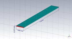
This filter’s RF performance with respect to S-parameters is shown in Figure 9. The insertion loss compared to the pure metallic waveguide counterpart is increased by an amount of about 0.3 dB. Return loss is better than 22 dB. As with the iris-based implementations, the dimensions are reduced by a factor of 10 in the vertical dimension and by a factor of 2.5 in the horizontal dimension.
Then, as in the design procedure followed for the H-plane iris-based implementation, the transverse walls of the metallic post-based waveguide are replaced by proper ground vias (Fig. 10).
The diameter of the posts is d = 0.1 mm, and the pitch is p = 0.2 mm. To obtain these values for the via diameter, we employed pitch-optimization techniques to obtain the best possible S11 in the passband as well as the best rejection for the out-of-band areas. The tuning posts inside the SIW structure are placed symmetrically and their diameter is 0.15 mm. The RF performance of the 3D geometry of Figure 10 appears in Figure 11. The dimension of this filter implementation compared to the H-plane iris based is smaller by about 0.9 mm.
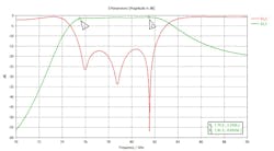
Comparing Figures 9 and 11 shows that the filter’s insertion loss has increased by 0.3 dB at mid-band. Although the return loss is affected, it remains well above 15 dB. Next, we implement the microstrip-to-SIW transition to finalize the design (Fig. 12).
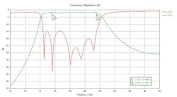
If we compare Figures 10 and 12, the additional length for each of the microstrip-to-SIW transitions is about 1.45 mm. Again, the simple tapered type of transition makes for the easiest fabrication.2 Figure 13 shows the RF performance of the final geometry shown in Figure 12. While the insertion loss is increased at mid-band by 0.5 dB compared to the non-transition case, the return loss and the out-of-band rejection are unchanged.
Conclusions
Our simulations show that metallic-type filters offer far better performance compared to their planar-technology counterparts as expected. Specifically, the microstrip filter delivers the worst performance due to radiation effects that exist in microstrip-technology implementations.
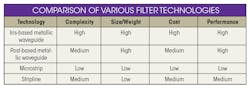
The table compares the various filter technologies in terms of manufacturing complexity, size/weight, cost, and RF performance. The lowest cost—and lowest performance—is found in the microstrip implementation, while the best performance at higher cost comes with the metallic waveguide filters.
In general, depending on the application, different approaches offer advantages and disadvantages.
Acknowledgment
The author wishes to acknowledge the staff of the School of Electrical and Electronics Engineering, WAVECOMM Laboratory of the University of West Attica for their support in preparing the article.
References
1. Xiao-Ping Chen, Ke Wu,” Substrate Integrated Waveguide Filter: Basic Design Rules and Fundamental Structure Features,” IEEE Microwave Magazine, July 2014, Montreal Polytechnic.
2. Ruey-Beei Wu, et al, “Design and Modelling of Microstrip Line to Substrate Integrated Waveguide Transitions,” National Taiwan University, April 2010, chapter in book Passive Microwave Components and Antennas.
3. Elena Diaz Caballero et al, “Efficient design of substrate integrated waveguide filters using hybrid mom/mm analysis method and efficient rectangular waveguide tools,” September 2011, IET Microwave Antennas and Propagation.
4. Muhammad Imran Nawaz et al, “Substrate Integrated Waveguide (SIW) to Microstrip Transition at X-Band,” Northwestern Polytechnical University, Proceedings of the 2014 International Conference on Circuits, Systems and Control.
5. Marcelino Armendariz, “Tunable Substrate Integrated Waveguide Filters implemented with pin diodes and RF MEMS switches,” Master’s Thesis, Texas A&M University, December 2010.
About the Author
Dr. Yorgos E. Stratakos
Faculty of Engineering, Department of Electrical and Electronic Engineering, University of West Attica
Yorgos E. Stratakos earned his diploma in Electrical and Computer Engineering in 1992 from National Technical University of Athens, and his PhD degree from the same university in 1995. He is a senior researcher on the faculty of Electrical and Electronics Engineering of the University of West Attica. His main research interests are RF and microwave design of analog passive and active circuits and systems.
