Millimeter Waves Enhance Military Projects
This file type includes high resolution graphics and schematics when applicable.
The spectrum congestion in the lower gigahertz region has caused many industries to seek technology solutions in the millimeter-wave spectrum. In fact, technology developments for millimeter-wave solutions in sensing and telecommunications have encouraged millimeter-wave research and development in almost every industry. Specifically, the military and aerospace industries are looking to millimeter-wave technology to increase connectivity and sensing for the next generation of tactical networks, security, electronic warfare (EW), and even active denial systems. This interest is being met with sponsored initiatives or product developments from military organizations, such as the Defense Advanced Research Projects Agency (DARPA), Air Force Research Laboratory (AFRL), and many military/security contractors.
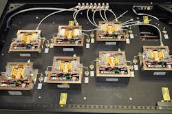
For its part, the AFRL—a dedicated organization within the United States Air Force—is tasked with developing warfighting technologies in the areas of air, space, and cyberspace. To meet these goals, the AFRL is delving into millimeter-wave technologies including high-power transmit sources, low-noise receivers, control component technologies, and multi-beam transmit arrays. The laboratory’s goal is to enable the Air Force to address the latest in increased bandwidth, data rate, and linearity requirements, thereby enhancing EW and communications systems with millimeter-wave technology (Fig. 1).
“Many of the components we currently work with and will be working with in the future use the benefits of shorter wavelengths to provide an advantage with compact solid-state and vacuum circuits,” states Lewis Kahias, Aerospace Components Technologies Division Principle Engineer for AFRL. “We are looking at opportunities that millimeter waves provide in terms of additional frequency spectrum. In general, we feel that moving up in frequency, whenever possible, will bring additional opportunities with higher data rates and more spectrum to work with.”
By taking advantage of the more compact solid-state and vacuum components available with millimeter-wave technology, the AFRL may be looking to reduce the size and weight of deployed systems. Of course, enabling such developments requires the use of solid-state transistor technologies, such as gallium nitride (GaN) and indium phosphide (InP). Innovative millimeter-wave vacuum-tube electronics also must be developed, which can handle high power and thus exceed the performance of traditional coupled cavity vacuum electronics.
Kahias comments, “We are developing vacuum electronic devices (VEDs) mainly for their power-level capability. With vacuum electronics, we can do extremely high-power electronics—and it generally doesn’t matter if it’s lower frequencies or millimeter wave. In general, vacuum electronics provide much higher power than solid-state electronics. In a lot of our efforts, we are expecting hundreds of watts of power from VEDs, as opposed to tens of watts from solid state. Solid-state electronics do have advantages with SWaP. We expect low-cost performance from a lot of platforms, so solid-state electronics have a niche with low-power performance.”
In terms of millimeter-wave semiconductor material, GaN is increasingly attracting interest for high-frequency and wide-bandwidth power electronics. Its high power density and high breakdown voltage make it well suited for such applications. For mission-critical applications, the robustness of the device is considered as critical as its performance. While GaN carves its niche, InP technologies are mainly being pursued for low-power and receive devices that require extremely linear and low-noise properties. Although gallium-arsenide (GaAs) technology may not be considered a fit for the latest military applications, it may still find a niche in lower-millimeter-wave, low-power applications.
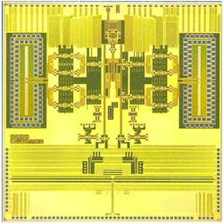
All new technology approaches come at the cost of substantial research, which must be done to overcome challenges and limitations. Generally, these higher-frequency electronic materials degrade in performance and efficiency as frequency increases. The added challenge of losing efficiency at millimeter-wave frequencies is managing thermal dissipation and reliability in both solid-state and vacuum electronics in much-reduced dimensions. Modeling these technologies also is a challenge, as no accurate models exist that can predict design performance for high-heat, high-frequency, and small-size compact devices. Fabrication yields and thermal and mechanical reliability issues also increase design complexity while limiting performance predictability. As a result, rigorous testing at a statistically significant level is necessary to produce viable models and reliability data (Fig. 2).
This file type includes high resolution graphics and schematics when applicable.
Device and Circuit Advances
This file type includes high resolution graphics and schematics when applicable.
Of particular interest to the AFRL is the development of several key components, such as ultra-wideband, agile, and survivable photonic RF receiver front ends. The goal of such front ends is to perform with enhanced receiver dynamic range and signal suppression while boasting compact up/downconversion electronics, which would support the use of photonic transmission lines as opposed to less efficient coax. Linearity and efficiency are critical for high-power, solid-state power amplifiers and drivers. As a result, current research aims to increase the linearity and efficiency of these amplifiers.
In addition, increasing the efficiency of wideband VEDs would help to reduce thermal stress, decrease system size, and lower the power budget for these devices. According to Steve Hary, Aerospace Components Technologies Division Principle Engineer for AFRL, “We are looking at using photonic technologies for broadband and low-loss signal transmission to overcome high losses from traditional microwave transmission lines, like coax. Other focus areas include advances in high-density packaging, such as 2D and 3D packages. As we pack things more densely with 3D technologies, we will need more advanced packaging and thermal-management techniques.”
To enable the latest in solid-state and vacuum-based millimeter-wave components and systems, several advances in device/circuit designs are needed. Also in demand is power-combining circuitry as well as higher-performance designs that are more linear, efficient, and wider bandwidth. The assembly, modeling, design, and process for manufacturing these devices also must be improved to meet yield, performance, and reliability requirements. To enable the photonic transmission-line systems, for example, advances are centering on photonic receiver components that support low-loss, millimeter-wave multi-beam transmit arrays and signal detectors over wide bandwidths.
To promote such evolution, the Manufacturing and Industrial Technologies Directorate (a section within the AFRL) has made investments in GaN fabrication technology. Its plan is to enhance the millimeter-wave development goals of the AFRL. It already is making progress, as evidenced by the $9.7-million agreement that the directorate entered into with RFMD to produce and transfer 0.14-μm GaN monolithic-microwave-integrated-circuit (MMIC) technology. The GaN MMIC technology will be produced on 6-in. scaled wafers with RFMD’s 6-in. GaN-on-Silicon Carbide (SiC) manufacturing line. This fabrication technology could enable GaN MMICs that operate beyond 100 GHz and enable new technologies for radar, military communications, and commercial applications using millimeter waves for telecommunications.
With the move to a 6-in. wafer, this process could provide up to 2.5 times more usable space over standard 4-in. GaN wafer processes. That translates into an increased number of GaN MMICs per wafer. The price of these ultra-wide-bandwidth, high-frequency, and high-power technologies could make some applications more accessible for commercial and military applications. RFMD is developing this technology for mass production in its US-based open foundry.
DARPA is another defense-oriented technology sponsor that is actively pursuing millimeter-wave technology for military applications. Recently, DARPA announced a prototype developed with Northrop Grumman Aerospace Systems. They demonstrated a complete system-on-a-chip (SoC) transmitter—made completely from silicon—that operates at 94 GHz (Fig. 3). This prototype hails from the Efficient Linearized All-Silicon Transmitter IC (ELASTx) program, which was developed to enable compact and high-data-rate millimeter-wave wireless communications that are smaller, lighter, higher performing, and less expensive. As opposed to GaAs or GaN millimeter-wave SoCs, an all-silicon SoC would be cost effective for a wide range of applications.
Another benefit of using all-silicon technology is the ability to design RF and digital circuitry in the same IC. This approach opens many doors to developing highly refined digital-control circuitry that can enhance the raw performance of RF designs. Embracing this concept, the digitally assisted power amplifier on the SoC transmitter can dynamically adjust the amplifier's key parameters to adapt to different signal requirements. With the ability to use real-time optimization for power, linearity, and efficiency, many tactical-network-based systems could be rapidly and efficiently implemented. Various aerospace and space applications, such as satellite communications for ground troops, could be enabled by the breakthroughs associated with this technology.
DARPA also is looking to advance the frontline soldier’s tactical capabilities via millimeter-wave-based mobile wireless hotspots, which will be mounted on unmanned-aerial-vehicle (UAV) platforms (Fig. 4). The goal of this technology initiative is to deploy a 1-Gb/s communications backbone to warfighting units in even the most remote environments. To enable this system, steerable millimeter-wave antennas, low-noise amplifiers, and efficient/higher-powered power amplifiers are being investigated.
Such devices are critical to enabling the low size, weight, and power (SWaP) performance targeted by this project. In the project’s second phase, L-3 Communications and FIRST RF will lead teams to enable this development. The project details a lightweight pod to be mounted on an SRQ-7 Shadow UAV. It will weigh under 20 lbs. while measuring less than 8 in. wide and consuming less than 150 W.
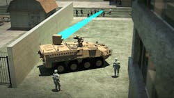
As these examples have shown, the majority of military applications have explored using millimeter waves as an enhancement technology. However, the U.S. Army Armaments Research Development and Engineering Center is collaborating with the Department of Defense Non-Lethal Weapons Program to develop a millimeter-wave-based solid-state active denial technology (SS-ADT). The SS ADT uses a 95-GHz steerable array that projects high-powered waves toward people in an undesired location (Fig. 5). By their nature, the 95-GHz waves theoretically allow only limited penetration (up to 1/64th of an inch into the skin). Although the body’s water molecules and nervous system would be heated and disrupted by the millimeter-wave radiation, no permanent injury would supposedly occur as long as people were only exposed to minor doses.
This file type includes high resolution graphics and schematics when applicable.
Imaging Applications
This file type includes high resolution graphics and schematics when applicable.
Millimeter-wave technology already is established in imaging security applications, such as airport screening equipment. Radio Physics Solutions, for example, produces a Millimeter Radar Threat Level Evaluation (MiRTLE) unit that is designed to detect concealed threats at ranges of several to tens of meters. The technology works by using low-power, ultra-wideband millimeter-wave illumination to capture and analyze reflected waveforms. The radar signatures for concealed weapons and explosives differ considerably from the signatures of casual items. As a result, detection algorithms can be used to analyze the specific reflected signals of each object to detect threatening objects. Given the power and algorithm methods behind this detection approach, it could allow for a less invasive and safe way of scanning many people and objects from longer ranges.
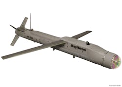
Military contractors, such as Raytheon, also are using millimeter-wave technology for imaging applications that extend the resilience of their airborne deployed bombs (Fig. 6). The Small Diameter Bomb II (SDB II) uses a tri-mode seeker comprised of a millimeter-wave radar, uncooled infrared (IR) imager, and digital semi-active laser sensor mounted in tandem on the same gimbal. The integrated seeker can fuse the targeting information between all three modes, which enhances the weapon’s ability to engage fixed, relocatable, or moving targets even in adverse weather conditions.
Here, the millimeter-wave radar enables the seeker to image effectively even when faced with a lot of debris, low visibility, low reflectivity, and dusty/sandy environments. The ability of millimeter waves to penetrate (or suffer limited attenuation) in these environments makes this technology a key component of all-weather and day/night visibility. Yet millimeter-wave technology has a drawback: its susceptibility to attenuation under moist atmospheric conditions, such as rain, fog, or high-humidity environments.
As military interests continue to raise investments in millimeter-wave technology, the challenges and cost concerns associated with implementing these systems will diminish. When the SWaP benefits of millimeter-wave technology can be realized, the unique and versatile application of millimeter-wave energy could lead to more advances in security, imaging, and communications. As millimeter-wave technology development increases for military applications, the commercial sector will benefit from the investment in enabling technologies. In a not too far-flung future, there may be readily available millimeter-wave wireless data for cell phones (5G, perhaps) with aerial drones supporting mobile millimeter-wave hotspots.
This file type includes high resolution graphics and schematics when applicable.
About the Author
Jean-Jacques DeLisle
Jean-Jacques graduated from the Rochester Institute of Technology, where he completed his Master of Science in Electrical Engineering. In his studies, Jean-Jacques focused on Control Systems Design, Mixed-Signal IC Design, and RF Design. His research focus was in smart-sensor platform design for RF connector applications for the telecommunications industry. During his research, Jean-Jacques developed a passion for the field of RF/microwaves and expanded his knowledge by doing R&D for the telecommunications industry.


