RF Reality in the Smart Home
What you'll learn:
- Why multi-protocol smart-home devices that pass lab tests can still fail in real RF environments.
- How antenna placement, isolation, impedance matching, and enclosure materials directly affect range, reliability, and battery life.
- A practical, repeatable RF design flow to ensure robust coexistence and performance in dense, real-world home deployments.

Smart-home products are rapidly evolving from single-radio nodes into dense, multi-protocol systems that must support Wi-Fi, Thread, Bluetooth Low Energy (BLE), and often sub-GHz or UWB within a single, highly constrained enclosure.
While Matter has accelerated interoperability across ecosystems, it’s also increased the number of active radios operating within the home (Fig. 1). The result is a growing disconnect between passing protocol tests and delivering reliable RF performance in real houses.

Devices that function correctly in controlled lab environments can struggle once deployed into RF-dense homes. Interoperability may be addressed at the software layer, but reliability is still governed by physics. That constraint becomes more significant as wireless fragmentation converges within the home, with multiple protocols and spectrum bands now coexisting within the same device.
Fragmentation Comes Home: Multi-Protocol by Default
The typical smart-home device no longer supports a single connectivity option. Instead, it may combine Wi-Fi (2.4 GHz, 5 GHz, and increasingly Wi-Fi 6), Thread, BLE, and sometimes sub-GHz connectivity or UWB positioning within a single compact enclosure.
Much of this activity occurs in the unlicensed spectrum, particularly the crowded 2.4-GHz band. While protocol designers have developed coexistence strategies at the MAC layer, physical-layer coexistence remains a separate challenge.
In some multi-protocol modules, a single device may integrate three separate antennas within a confined footprint. Achieving sufficient isolation between these elements — while preserving radiation efficiency — becomes non-trivial. When multiple radios share common ground structures and confined enclosure volume, mutual coupling can quickly erode link margin.
These integration pressures are compounded by spectrum choices. Certain applications, including smart meters and heating systems in Europe, are increasingly moving toward sub-GHz bands such as 868 MHz.
Lower frequencies improve penetration through walls, but they require physically larger antenna structures, greater clearance from metal enclosures, and more substantial ground planes. The mechanical- and industrial-design implications can dominate enclosure and layout decisions.
The Real RF Environment of a Matter-Enabled Home
Unlike anechoic chambers or simplified bench setups, real homes are electrically complex environments. Walls, reinforced concrete, appliances, and metal fixtures introduce attenuation, reflection, and multipath propagation, causing fading that varies with small positional changes. At 2.4 GHz, congestion from neighboring networks, legacy routers, and consumer electronics further raises the noise floor.
Developers sometimes assume that limited coverage is acceptable in a domestic environment, and that a few meters of range will suffice. In practice, once installed in a real home, devices operate in electrically complex surroundings with multiple active transmitters and unpredictable interference. Marginal lab performance can quickly turn into practical problems — blinds that fail to respond, sensors that drop offline, or hubs that lose connection stability.
In some applications, the consequences extend beyond inconvenience. EV chargers that rely on reliable smart-meter connectivity to access optimal tariffs can directly affect a homeowner’s electricity costs. In these cases, unreliable RF performance could translate directly into lost tariff savings and frustrated customers.
Why Smart-Home Designs Still Fail in the Field
Despite advances in chipsets and protocol stacks, many failures can be traced to basic RF integration issues.
A common issue is insufficient antenna-to-metal clearance. Enclosure walls, internal shielding, mounting hardware, and even decorative metallic finishes can detune an antenna, reducing efficiency and shrinking effective range. The impact may not appear during early validation, but it often emerges during certification or field deployment.
Impedance mismatch is another overlooked factor, translating into increased current draw and shortened battery life in smart-home devices.
Time pressure often compounds these risks, with compressed testing cycles in fast-moving markets. Environmental validation and full coexistence evaluation can be deferred, only for customer complaints to surface later. Many late-stage redesigns originate from architectural RF decisions made early in the program, long before performance problems become visible.
Antenna and Front-End Strategies for Coexistence in Real Smart-Home Form Factors
Mitigating these risks requires deliberate antenna and front-end architectural decisions made with the final enclosure and operating environment in mind.
Antenna topology is a key consideration (Fig. 2).
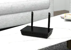
Shared antenna approaches can reduce cost and conserve space, but they introduce additional filtering, switching complexity, and isolation challenges. Dedicated antennas per radio may improve robustness, although they demand careful spatial planning within constrained enclosures and increase pressure on PCB real estate and mechanical design.
Physical integration is equally important. Adequate antenna-to-metal clearance, from enclosure walls and internal shields to battery cans and other conductive elements, is one of the most effective safeguards against performance degradation. These constraints become even more pronounced at lower frequencies, such as 868 MHz, where antenna size increases and interaction with ground structures becomes more significant.
When multiple radios coexist within a confined footprint, isolation must be designed in from the outset. Antenna spacing, orientation, ground strategy, and filtering all influence coexistence performance. In dense gateways or hubs operating simultaneous radios, unintended coupling can degrade receiver sensitivity or introduce desensitization risks if not carefully controlled.
Impedance matching is equally important to overall system performance. The effectiveness of the impedance match has a direct impact on radiation efficiency and the load presented to the RF front end.
Poor matching increases return loss, reducing effective radiated power and lowering received signal strength integration (RSSI) at the peer device. Reduced link margin drives retransmissions and higher transmit duty cycle. In battery-powered smart-home devices, this translates directly into higher average current consumption and reduced operating life — a predictable consequence of suboptimal antenna integration.
Form factor further shapes these tradeoffs. Mains-powered devices may experience conducted noise and grounding interactions. Retrofit products, such as smart switches installed in metal backboxes, operate in RF-hostile environments with limited clearance. Gateways and hubs must balance antenna isolation against thermal constraints and compact industrial design requirements.
In practice, RF performance reflects how antenna choice, enclosure design, PCB layout, and power architecture interact in the finished device. Addressing these constraints requires early coordination between RF, mechanical, and industrial design disciplines.
A Repeatable RF Design Flow for Smart-Home Products
As smart-home devices grow more complex, reliable wireless performance requires a disciplined RF design process.
The process begins with early RF engagement, ideally before enclosure materials, PCB stackups, and industrial design are frozen. Antenna location, ground clearance, and proximity to noise sources should be treated as primary architectural decisions.
Next comes context-aware antenna selection. Designers must evaluate not only frequency band and efficiency targets, but also enclosure materials, device placement expectations, and multi-radio interaction within the final form factor (Fig. 3).
The next step is iterative validation, combining simulation with empirical measurement. Modelling tools support early exploration, but enclosure effects and coupling paths must be confirmed through representative measurement.
Final antenna tuning is carried out with the complete mechanical and electrical system in place, including cabling, power architecture, and sources of conducted or radiated noise. Tuning an isolated PCB rarely reflects the behavior of the finished product.
Pre-certification RF checks should then confirm link margin, coexistence robustness, and receiver sensitivity under realistic conditions before formal compliance testing gets underway. This reduces the risk of repeated certification cycles and costly redesigns.
Online integration and simulation tools can support this methodology. Manufacturers such as Taoglas provide cloud-based design platforms to guide antenna selection, placement, and optimization.
Taoglas’ new AI-driven Antenna Product Recommendation Engine, for example, leverages application parameters to accelerate initial antenna selection, reducing iteration time while still requiring engineering validation. Embedded within a structured RF design flow, such tools reduce risk without sacrificing development speed.
Designing for Houses, Not Chambers
Matter has simplified interoperability, but it hasn’t simplified RF physics. The modern smart home is a dense and dynamic RF environment, where enclosure materials, device placement, congestion, and multi-radio interaction all shape performance.
Reliable smart-home products depend on early, disciplined RF architecture decisions. Late-stage tuning can’t compensate for structural integration shortcomings. A well-executed RF design provides predictable performance in real deployment environments, giving developers, installers, and end users confidence that connected devices will operate as intended.
About the Author

Baha Badran
Global Head of Engineering, Taoglas
Baha Badran has over 20 years of experience in RF, antenna design and product development across thousands of projects. He leads a strong team of 60 world-leading engineers at Taoglas.
Baha joined Vertu/Nokia as an Antenna Engineer in 2007, working on antenna design and development for luxury mobile phones. He later advanced to the role of Senior Antenna Design Engineer, leading antenna development for various Vertu products. In 2015, he joined EDMI Limited as an RF Engineer, before transitioning to EDMI Europe Limited in 2016 as the Lead Hardware Engineer. Since 2017, he’s been working at Taoglas, starting as a Senior Antenna Design Engineer and progressing to the role of Engineering Manager (EMEA) and then Global Antenna Technology Director. Currently, he serves as the Global Head of Engineering at Taoglas.
Baha Badran holds a Bachelor of Engineering (B.Eng.) degree in Electrical, Electronics, and Communications Engineering from An-Najah National University, which he completed from 2000 to 2005. Subsequently, he pursued a Master's degree in Personal Mobile and Satellite Communications from the University of Bradford from 2005 to 2006.
