Silicon Paves Way for Photonics Expansion
Silicon has long been the building-block material of choice for analog and digital semiconductors, but it appears to be gaining favor for photonics components, as well. Silicon offers the highest crystalline quality and lowest cost per area of any semiconductor wafer material, along with compatibility with mature electronics integrated-circuit (IC) processes, such as silicon CMOS circuits.
It’s no wonder than major IC suppliers would be interested in pursuing photonics devices on silicon substrates, provided that the performance meets all requirements. For some time, silicon photonics devices from leading suppliers such as Intel have supported data rates of 100G, with current developing efforts progressing towards data rates of 400G.
Silicon semiconductor wafers are typically 6 to 12 in. in diameter. Fortunately, photonics devices can be fabricated in foundries using standard silicon CMOS fabrication techniques, allowing for cost-effective manufacturing and production. Among the many components fabricated on silicon for photonics systems are optical waveguides and various photonic integrated circuits (PICs), used to form planar lightwave circuits (PLCs) on a silicon wafer.
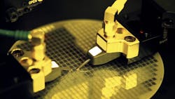
Silicon wafers have long supported the fabrication of analog and digital circuits, but have also become the substrate of choice for photonics devices and ICs. (Courtesy of NeoPhonics)
The various devices are used with fiber-optic cables to achieve attenuation, splitting, filtering, multiplexing/demultiplexing, and high-speed switching functions in support of fast, reliable optics-based data communications systems. Some are long distance and some travel only within the confines of a system or a single circuit board. But the technology is sound, and silicon semiconductors have shown that they are capable not only of high-speed digital signal processing but photonics signal processing as well.
A recent report from IndustryARC focusing on silicon photonics markets, “Silicon Photonics Market: By Components and By Application (Aerospace & Defense, Healthcare, Telecommunications, Consumer Electronics, Industrial Automation and Others)—With Forecast (2016-2021),” predicts strong growth for silicon photonics markets through the next five years. In addition to current devices, it projects a growing number of ICs and devices that integrate several technologies on a single chip, made possible by the common silicon substrate.
Such circuits could include photonics devices, memory, microprocessors, digital signal processing, and even RF/microwave transceiver circuitry, fabricated on the same silicon wafer and integrated within a common package for ease of use in an application.
Silicon photonics is currently a wide-ranging market space, including not only the familiar high-speed telecommunications applications but also infrared (IR) lenses and detector and imaging elements in digital cameras. Application areas include commercial and consumer markets, as well as industrial and military users.
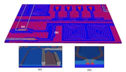
The silicon photonics test die show (a) a Mach-Zehnder modulation and (b) a directional coupler. (Courtesy of Coventor)
Optical detection and imaging technologies work side by side with millimeter-wave radar systems in modern automotive safety systems, presenting the unique opportunity to have optical waveguide and millimeter-wave waveguide within the same platform, supporting optical and electromagnetic (EM) technologies. Of course, the same can be said of a number of aerospace and defense-related applications, including those for electronic warfare (EW) and electronic counter-measures (ECM).
Integrated photonics technology has the support of many industry groups—among them the American Institute for Manufacturing Integrated Photonics (AIM Photonics), a public-private partnership. The organization recently announced the addition of device modeling specialist Coventor as a member, bringing its expertise in physics-based, three-dimensional (3D) modeling to the world of integrated photonics design.
Managed by SUNY Polytechnic Institute, AIM Photonics is attempting to build a membership that includes the most innovative technology companies in the U.S. “Building upon our commercial experience in the semiconductor industry, we see our membership in AIM Photonics as essential to our mission in supporting the design and manufacturing of next generation, photonic integrated components,” said Michael Jamiolkowski, Coventor’s president and CEO.

About the Author
Jack Browne
Technical Contributor
Jack Browne, Technical Contributor, has worked in technical publishing for over 30 years. He managed the content and production of three technical journals while at the American Institute of Physics, including Medical Physics and the Journal of Vacuum Science & Technology. He has been a Publisher and Editor for Penton Media, started the firm’s Wireless Symposium & Exhibition trade show in 1993, and currently serves as Technical Contributor for that company's Microwaves & RF magazine. Browne, who holds a BS in Mathematics from City College of New York and BA degrees in English and Philosophy from Fordham University, is a member of the IEEE.
