Leveraging advanced gallium-nitride (GaN) device technology, imec has developed a metal-oxide-semiconductor high-electron-mobility transistor (MOSHEMT) enhancement-mode (E-mode) semiconductor process on silicon (Si) substrate. The advancement, which promises high output-power levels at microwave frequencies, is expected to target high-power mobile communications devices like those required in 6G networks.
The GaN-on-Si enhancement-mode MOSHEMT process yielded a device with more than 0.5 W (+27.8 dBm) output power and 66% power-added efficiency (PAE) at 13 GHz. It operates on +5 V DC bias and features a robust 1-W/mm periphery (as). The device technology boasts low contact resistance of 0.024 Ω-mm, as imec demonstrated with a separate device module fabricated with the technology. Results were presented at the 2025 Symposium on VLSI Technology and Circuits (June 8-12, 2025, Kyoto, Japan).
Although current mobile communications networks occupy frequencies and bandwidth below 6 GHz, ever-increasing numbers of users are feeding a need for additional bandwidth and higher frequencies. The GaN-on-Si MOSHEMT device technology is well-suited to the 6G FR3 frequency band between 7 and 24 GHz.
Though GaN device technology, attractive for its high power density, isn't new, it's been costly to fabricate high-power devices on silicon-carbide (SiC) substrates used in cellular communications base stations. GaN-on-Si promises to be more affordable than GaN-on-SiC devices while delivering equivalent power levels with higher efficiency.
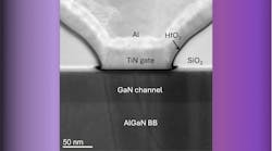
The GaN-on-Si E-mode results obtained by imec were for a single MOSHEMT device with eight-finger gate layout to achieve the target output-power levels (see image above). The device architecture combines a gate recess technique, to shift the device into E-mode, with an InAlN barrier layer to enhance the performance of a thinned channel.
Alireza Alian, Principal Member of Technical Staff at imec, noted, “Reducing contact resistance is crucial for pushing output power while keeping efficiency high.” He added, “Our next step is to integrate this contact module into the E-mode transistor and validate the expected gains in power and efficiency, bringing the device closer to real-world 6G applications.”


