Classic SiP Tech Repels Modern Threats
Download this article in PDF format.
Choice of packaging technology can often determine an electronic technology’s ultimate effectiveness in a defense-related application. Once considered highly advanced, system-in-package (SiP) technology is no longer at the forefront of microelectronic packaging.
But, while other applications may seek to leverage the latest and greatest packaging technologies, military system architects cannot leverage new packaging technologies without clear evidence of military-grade reliability. In fact, by using a four-pronged approach, it is possible to modernize a proven, existing packaging technology—SiP—to power military applications in the most threatening environments.
SiP technology is still a valid approach for miniaturizing defense microelectronics, but other packaging options now crowd the scene (Fig. 1). Semiconductor manufacturers and outsourced assembly and test (OSAT) providers have made tremendous progress in the commercialization of through-silicon-via (TSV) technology to interconnect multiple devices in compact form factors. The technology has matured sufficiently such that logic, memory, RF devices, sensors, and passive components are often integrated in a single package. While it would appear that the defense community would widely adopt TSV technology as its next packaging technology, there are still strong needs for SiP devices.
1. The small size of modern SiP technologies allows for extreme miniaturization of digital microelectronics capable of handling defense operating temperatures and conditions.
The performance benefits of TSV technology are well-established at commercial operating temperatures (0° to +70°C). Yet, military missions are not restricted to such a narrow operating temperature range.
In addition to temperature extremes—from −55 to +125°C—military electronics are also exposed to harsh thermal shock conditions from one temperature extreme to the other. Typical operating environments also include high altitudes, severe mechanical shock, vibration, and exposure to moisture. With all of these less-than-ideal operating conditions, military microelectronics are expected to perform flawlessly for years and even decades while being subjected to these operating environments.
Yes, the defense community must embrace commercial technologies to support military interests. However, this cannot be done without caution. For a military system architect, the decision to implement a new technology can lead to catastrophic consequences. Thus, the need arises for systematic evaluation of new technologies in realistic application environments. Furthermore, the perfect storm of worst-case environmental conditions must be an evaluation criterion. A quick review of the literature using any search engine quickly reveals that TSV technology has not yet matured to the levels required for predictable, long-term reliability in military application scenarios.
Before proceeding further, it is worthwhile discussing the spectrum of possibilities regarding the concept of an SiP device. Many manufacturers refer to an SiP device as a two-dimensional (2D) array containing a central processing unit (CPU) and memory, where interconnections between the devices are optimized for performance.
Best-of-breed SiP manufacturers will leverage three-dimensional (3D) stacking technologies (not to confused with TSV technology) to minimize the 2D footprints of their devices (Fig. 2). Even fewer suppliers can apply multiple device interconnection technologies, such as wire bonding, surface-mount devices, and flip-chip devices, on the same design. Unlike a packaged device created with TSV technology, SiP devices can be rapidly prototyped and customized for specific program requirements.
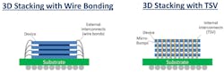
2. The 3D stacking in modern SiP enclosures makes it possible to squeeze a great deal of functionality within a small package size without sacrificing reliability.
While TSV technology is not suitable in forward-deployed military applications, it is worth questioning the fundamental assumption that tried-and-true SiP technology is no longer valuable for leading-edge defense applications. How can SiP technology be modernized to deliver the performance requirements demanded by our modern military forces? Four new SiP attributes are proposed: agile customization, advanced thermal management, embedded security, and trusted manufacturing.
Agile Customization
In years past, the defense industry converged on a single processor, the PowerPC, for military applications. Device scaling according to Moore’s Law has enabled tremendous processing advances while reducing size, weight, and power consumption since the PowerPC was state-of-the-art.
Today, military system architects can choose from a wide range of processors and field-programmable gate arrays (FPGAs) to address different processing requirements. There is no universal combination of processor and memory that addresses every military application at present. Just as TSV technology can incorporate additional functionality beyond a processor and memory, SiP technology also embeds sensors and passive components, in addition to power-management circuitry.
Modern SiP devices must be developed by manufacturers capable of supporting rapid prototyping for new programs while sustaining production of a wide variety of legacy devices. Time to market, from concept development to production, must occur in less than one year to meet aggressive program schedules. The “one-size-fits-all” approach of the past must be replaced by agile customization for tomorrow.
Thermal Management
Modern military computing systems process multiple, parallel data streams from a number of different sensor systems. Design rules for each device technology node continue to shrink. The processing demands placed on these compact devices are resulting in higher power densities, increasing the challenges for effectively dissipating the amount of heat generated. In applications where space constraints do not exist, discrete devices can dissipate heat via any combination of radiation, conduction, and convection.
When these devices are embedded within a ruggedized SiP device, thermal-management considerations cannot be avoided. Further complicating this scenario, it is distinctly possible that more than one processor, whether FPGA or GPU, must be embedded within the packaged device (Fig. 3).
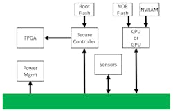
3. This block diagram is one example of the number of functions that can be contained in a miniature SiP housing.
Next-generation SiP technology requires the manufacturer to dissipate a minimum of 100 W power without negatively impacting size, weight, and power (SWaP) or performance. Advanced thermal and mechanical modeling using highly sophisticated design tools maximizes thermal performance of a packaged device. Predictable and reliable performance in environmental conditions simulating actual military environments is a prerequisite for SiP devices.
Embedded Security
Our military forces must maintain a strategic and tactical edge in global operations. The technology enabling these advantages must be protected at all costs. Yet it is unavoidable that many of the most advanced computing systems will be deployed in environments where platform capture is a possibility. Adversaries gaining access to these strategic technologies will leverage any tactic to understand the performance and construction of these devices, in addition to decrypting any stored data.
Although security features are typically not associated with SiP technology, embedding security within a SiP device is critical to protect the interests of our military forces. Achieving this ambitious goal of embedded security requires the intersection of two disciplines unfamiliar with each other: security architectures and microelectronics packaging. The typical defense microelectronics packaging supplier only achieves this objective through partnerships forged with security subject matter experts.
Trusted Manufacturing
Commercial microelectronics are manufactured in locations optimized to produce the highest volume of product per unit time with maximum cost efficiency. Nearly all electronic components today are manufactured outside the borders of the United States. As such, it is nearly impossible to guarantee that an adversary has not introduced bypass mechanisms into these devices to alter performance in life-or-death missions. Other supply-chain attacks may be more subtle. As an example, the introduction of counterfeit materials into the manufacturing process of a defense computing system can compromise mission performance.
Addressing the future needs of the defense market requires SiP manufacturers to take a holistic perspective to embedding trust within the cadence of daily operations. Supply-chain monitoring, particularly for critical components, ensures the authenticity of all procured parts.
The manufacturing environment must be monitored to make sure that manufacturing and quality procedures are rigorously followed without exception. The backgrounds of all employees directly or indirectly related to device manufacturing should be fully vetted. Finally, the network infrastructure containing valuable design and manufacturing records requires protection from cyberattacks through a vigilant cybersecurity program. The establishment of a trusted manufacturing center is not a trivial task, but manufacturers creating such centers of excellence will quickly realize the benefits.
By successfully incorporating agile customization, advanced thermal management, embedded security, and trusted manufacturing, SiP technology can be extended to address the requirements of modern military forces. Strategically designed enhancements based on application-specific requirements can deliver tangible benefits, as this example shows. Introducing these incremental innovations to proven technologies also offers affordability benefits, since there’s no need to replace existing design and manufacturing equipment.

