How to Achieve Ultra-Fast Power-Supply Transient Response in RF Apps
Members can download this article in PDF format.
What you’ll learn:
- Why fast power-supply load transient response is critical in RFSoC circuits.
- How to use pre-charge signals to drive regulators.
- Using active drooping circuits to minimize power-supply recovery time.
Signal processing units and system-on-chip (SoC) units usually possess abruptly changing load-transient profiles. This load transient will result in a disturbance on the supply voltage that’s critical in RF applications, as the clock frequency will be highly affected by the varying supply voltage. Thus, RFSoCs usually apply blanking time during the load transient.
In 5G applications, information quality is highly related to this blanking period during the transition. As a result, there’s an increasing need to minimize the load-transient effect on the power-supply side to improve the system-level performance for any RFSoC system. This article will introduce several methods used in RF applications to achieve fast transient response in a power-supply design.
Fast Transient Switching Regulators
One of the most straightforward methods to achieve fast transient power rails is to select regulators that feature fast transient performance. An example of such devices is ADI’s Silent Switcher 3 family of ICs, which offer exceptionally low-frequency output noise, fast transient response, low-EMI emissions, and high efficiency.
The regulators feature an ultra-high-performance error-amplifier design that can provide extra stabilization even with an aggressive compensation. Their 4-MHz maximum switching frequency enables the ICs to push the control-loop bandwidth to the mid-hundred-kilohertz range in a fixed-frequency, peak-current control mode. The table lists the Silent Switcher 3 ICs that designers can select to achieve fast transient performance.
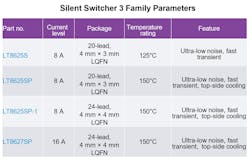
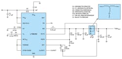
Figure 1 shows a typical power supply with a 1-V output based on the LT8625SP for a 5G RFSoC, which needs fast transient response and low ripple/noise level at the same time. The 1-V load consists of both transmit/receive-related circuits as well as local oscillators (LOs) and voltage-controlled oscillators (VCOs).
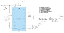
The transmit/receive loads see abrupt load-current change during frequency-division duplex (FDD) operation. At the same time, LOs/VCOs see a constant load but require critical high accuracy and low noise.
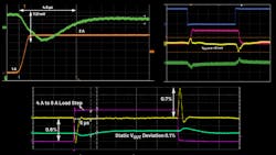
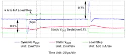
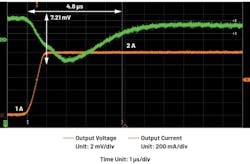
The high-bandwidth feature of the LT8625SP enables designers to power the two critical 1-V load groups from a single IC by separating the dynamic load and static load with a second inductor (L2). Figure 2 shows the output-voltage response with a dynamic load transient of 4 to 6 A. The dynamic load recovers within 5 µs with less than 0.8% peak-to-peak voltage, which minimizes the effect on the static load side with a less than 0.1% peak-to-peak voltage.
This circuit can be modified to accommodate other output combinations, like 0.8 V and 1.8 V, that can all directly supply the RFSoC load without the LDO regulator stage due to the ultra-low noise in the low-frequency range, low voltage ripple, and ultrafast transient response.
In time-division-duplex (TDD) mode, the noise-critical LOs/VCOs become loaded and unloaded together with the transmit/receive mode changes. Thus, a simplified circuit (Fig. 3) can be used, because all of the loads are dynamic in character while more critical post-filtering is required to maintain the low-ripple/low-noise feature for the LOs/VCOs.
Using a three-terminal capacitor in feedthrough mode achieves enough post-filtering with a minimized equivalent L that maintains a fast bandwidth for the load transients. The feedthrough capacitor, together with the remote-side output capacitors, forms two more LC filter stages. All of the inductances come from the equivalent series inductances (ESLs) of the three-terminal capacitor, which is very small and less harmful to the load transient.
Figure 3 also illustrates an easy remote-sensing connection for the Silent Switcher 3 family. Due to the unique reference generation and feedback technology, one only needs to Kelvin-connect the SET pin capacitor’s (C1) ground and the OUTS pin to the desired remote feedback point. No level-shifting circuits are needed for this connection. Figure 4 shows a 1-A load transient-response waveform with <5-μs recovery time and <1-mV output-voltage ripple.
Pre-charge Signals Drive Regulators
In some cases, the signal-processing unit is powerful with enough general-purpose I/Os (GPIOs), and because the transient event is predictable, the signal processing is well scheduled. This usually happens in some FPGA power-supply designs where the pre-charge signal can be generated to help power the supply transient response.
Figure 5 shows a typical application circuit using the pre-charge signal generated by the FPGA to provide a bias before the real load transition occurs. As a result, the LT8625SP can have extra time to accommodate the load disturbance without too large of a VOUT deviation and recovery time. The tuning circuit from the FPGA’s GPIO to the input of the inverter has been omitted since the pre-charge signal is acting as a disturbance on the feedback. The level is controlled at 35 mV.
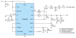
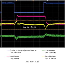
Moreover, to avoid the pre-charge signal effect on the steady state, a high-pass filter is implemented between the pre-charge signal and the OUTS pin. Figure 6 shows a load transient-response waveform of 1.7 to 4.2 A. The pre-charge signal is applied to the feedback (OUTS pin) ahead of the real load transient, achieving a recovery time of less than 5 µs.
Active Drooping on Circuit for Ultra-Fast Recovery Transient
In beamformer applications, the supply voltage changes constantly to accommodate different power levels. As a result, the accuracy requirement for the supply voltage is usually 5% to 10%.
In this application, stability is more important than the voltage accuracy, because a minimized recovery time during the load transient will maximize the data-processing efficiency. A drooping circuit is well-suited for this application because the drooping voltage will reduce or even eliminate the recovery time.
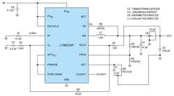
Figure 7 shows the schematic for an active drooping circuit for the LT8627SP. An extra drooping resistor has been added between the error amplifier’s negative input (OUTS) and the output (VC) to maintain a steady-state error in the feedback control loop during the transient.
The drooping voltage can be expressed as:
Whereas ∆VOUT is the initial voltage variation caused by the load transient, ∆IOUT is the load transient current, and g is the VC pin-to-switch current gain. When designing the drooping circuit shown in Figure 7, one should be aware of a couple of special considerations:
- The drooping current should not exceed the VC pin current limit. For the LT8627SP’s error amplifier output, limit the current to below 200 µA to avoid saturation; this can be achieved by changing R7 and R8 values.
- The drooping voltage needs to accommodate the output capacitance so that the voltage deviation during the transient is on a similar level of the drooping voltage to achieve minimum recovery time during the transient.
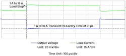
Figure 8 shows typical waveforms for the above-mentioned circuit during a load transient from 1 A to 16 A and back to 1 A. Note that the 16-A-to-1-A load-transient speed is no longer bottlenecked by the bandwidth, but rather by the minimum on time of the regulator.
Conclusion
The wireless RF field is becoming increasingly dependent on calculations and sensitive to the transient-response time due to the time-critical nature of the high-speed signal processing. System design engineers face challenges to increase the power-supply transient-response speed to minimize the blanking time. Based on the load conditions, special techniques and circuits can be applied to further improve the transient response.
About the Author
Xinyu Liang
Applications Engineering Manager, Analog Devices Inc.
Xinyu Liang is the applications engineering manager in the Industrial and Multimarket Group at Analog Devices focusing on power products. He received his Ph.D. degree in electrical engineering in 2018 from North Carolina State University and started his career at ADI in 2019 after graduation.
