Improving Wideband Multichannel Systems with IC Integration (Part 3)

Members can download this article in PDF format.
What you’ll learn:
- How FPGA utilization determines where to implement pFIRs.
- Higher FIR sample rates can overwhelm FPGA resources.
- Using hardened pFIRs in a digitizing IC delivers lower power consumption and less strain on FPGA DSP slices.
In Part 1 of this article series, we covered digital signal processing blocks as well as digital up/downconverter blocks. In Part 2, we covered programmable finite-impulse-response filters and achieving channel amplitude alignment and gain flattening in great detail. In this final installment, we’ll cover digitizing element resource consumption versus FPGA resource consumption, and then compare their power consumption.
Digitizing Element Resource Consumption vs. FPGA Resource Consumption
As discussed, on-chip hardened programmable finite-impulse-response filters (pFIRs) exist within the analog-to-digital converter (ADC) data path before the decimation stages. As we’ve shown, these pFIRs present users with significant application flexibility, but the pFIRs also allow developers to significantly reduce FPGA resources due to the feature offload to the digitizing IC itself.
The obvious question becomes: Why use the hardened pFIRs on the digitizing IC instead of within hardware-description-language (HDL) fabric on an FPGA? This can be answered in several parts: resource reduction, design complexity, and power consumption.
Resource reduction is an important topic regardless of focus area. In the case of the digitizing IC, hardened pFIR blocks are already created and placed. In an FPGA, a FIR filter can be built from DSP slices that contain specific FPGA fabric components intended for DSP functions. FPGA DSP slices are different than traditional logic gates, such as flip-flops, and count toward FPGA resource utilization separately.
To determine if the pFIRs should be used on either the digitizing IC or the FPGA, the utilization of the FPGA—specifically the DSP slice-utilization percentage—becomes paramount. As a point of comparison, the chosen VCU118 platform contains an XCVU9P Virtex Ultrascale+ Xilinx FPGA consisting of 6,840 DSP slices. While that’s a relatively large number of DSP slices, the number of channels also must be considered when determining how many filters are to be placed in the fabric.
To achieve that, the desired input sample rate of the filter must be known. Table 1 shows an estimated number of resources required when synthesizing an FIR design on the FPGA for several use cases that map to potential digitizing IC data-path configurations. These estimated number of resources for each filter comes from the Xilinx LogiCORE IP FIR Compiler 7.2 block summary.
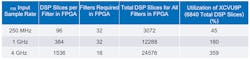
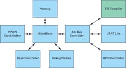
To view the summary, a filter was added to a simplified MicroBlaze design (Fig. 1) that was created in Xilinx Vivado Design Suite 2018.2. The 250-MS/s and 1-GS/s rates are situations where the FIRs would operate with decimated data from the converters, while the 4-GS/s case assumes that the data is input undecimated directly from the converter. Each FIR filter runs at 250 MHz to mimic the speed at which an FIR filter would operate if it were in the baseband data path and contains 96 16-bit reloadable coefficients.
Given the percentage utilization of the XCVU9P FPGA, it becomes clear that a larger FPGA such as the XCVU13P (with 12,288 DSP slices) must be utilized to contain all of the required filters. In the case of 4-GS/s FIR filters, it would take at least two of the XCVU13P devices to share the resource loading of every filter, which in turn increases the cost of the design. In contrast, all filters required for all 16 channels used on the hardened DSP pFIR implementation discussed in Parts 1 and 2 of the series are completely contained within the digitizing ICs themselves to achieve a simpler system-design approach.
Another major concern with the FIRs inside an FPGA is the design complexity associated with the high DSP slice-resource utilization. Consider how to build the filter. On silicon, the filter design is fixed in a single location in the chip, but the coefficients and weightings can be digitally altered, resulting in a relatively static implementation.
In an FPGA fabric, the FIR filter design routes those DSP slices in various regions of the chip. This means that as the filter grows or changes, more area of the FPGA is consumed and routing connections between DSP slices becomes more and more challenging. Secondly, the routing of the rest of the FPGA design can be impaired by expanding the FIR filter design, which may make timing-critical routing difficult, if not impossible, in certain situations.
Digitizing Element Power Consumption vs. FPGA Power Consumption
The general industry trend of increased converter sample rates and multichannel integration often leads a system architect to analyze the system power consumption when implementing DSP blocks in the overall design. Historically, these DSP blocks have been implemented with the use of programmable logic, such as is found within an FPGA. However, implementing configurable blocks within the FPGA can often create excess overall system power consumption.
To directly compare both systems, we created several simplistic reference designs for the VCU118 to determine the relative difference in power consumed by the FPGA-based filter approach in a realistic scenario. The VCU118 was chosen because, at the time, it had the most DSPs of any evaluation system directly provided and supported by Xilinx.
Based on the VCU118, we created two Vivado projects for each FIR input sample rate—one with filters and one without. For both the 250-MHz and 1-GHz cases, we inserted eight FIR filters into the design like that shown in Figure 1.
In the 4-GHz case, we inserted only two FIR filters into the design due to high resource utilization. We fed each filter using the output of the Xilinx LogiCORE DDS Compiler 6.0 block to ensure use of valid data. It also was important to note that we examined the RTL after synthesis to verify that filters remained in the design, making sure they weren’t optimized away. In the second design for each sample rate, the filters were removed, but all other IP blocks remained in place.
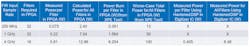
Once implemented, we booted the designs and took current measurements to create a relative power delta. By doing so, we isolated the additional power required by the filters. The current draw of the filters can be seen in Table 2 under the measured power per filter column. We then extrapolated the total power draw for all of the filters using the data collected for a limited number of filters in the design (eight filters for 250-MHz and 1-GHz cases and two filters for the 4-GHz case).
This delta was the basic unit of comparison, which was used to scale to different configurations that aren’t implementable with the VCU118, but possible with the digitizer IC. The authors believe it’s relatively fair or possibly advantageous toward the FPGA because a real system’s power draw is unlikely to scale linearly.
Lastly, we compared the results against the power estimates for various filter implementations generated from the Xilinx Power Estimator (XPE) tool.1 The power estimates are much higher than the extrapolated results, but this could account for the nonlinear increase in power because of the increased utilization.
To compare the power draw of the FIRs in the FPGA to that of the hardened pFIRs in the digitizer IC, we compared the measurements from the simple filter designs to the actual current draw of the multichannel system, which uses hardened pFIR DSP blocks on the digitizer ICs.
Including all of the front-end networks and clocking circuitry, the total system power consumption using the digitizer IC platform without the hardened pFIRs enabled is approximately 98.40 W. When all 16 hardened pFIRs are enabled, the total system power consumption using the digitizer IC platform is approximately 104.88 W. Therefore, the power-consumption delta of the hardened pFIRs applied in the multichannel platform is around 6.48 W total for all 16 receive channels on the digitizing IC system. The hardened pFIRs are receiving data from the ADCs directly and must run at the ADC sample rate (4 GS/s) for this present generation.
However, comparing this power consumption to what would be consumed by 16 4-GS/s FPGA FIRs is a bit unreasonable, because the resource utilization is impossibly high for a single Virtex Ultrascale+ series FPGA. Therefore, the 250-MS/s-rate FPGA FIRs are compared to the hardened 4-GS/s pFIRs, with Table 2 and Figure 2 showing that the power consumption of the 32 FPGA FIRs (16 I FIRs and 16 Q FIRs) is 2.40 W. The filters in the FPGA are running 16X more slowly than those in the hardened digitizer IC DSP blocks, but the FPGA still consumes 0.37X as much power as the hardened digitizer ICs.
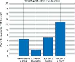
Comparing the 32 1-GS/s FPGA FIRs to the hardened 4-GS/s pFIRs, the FPGA FIRs draw about 7.04 W (which is already higher power consumption than the hardened pFIRs) while operating 4X slower than the hardened pFIRs. Comparing the 16 4-GS/s FPGA FIRs to the 16 hardened 4-GS/s pFIRs, the FPGA consumes 2X as much power with this system configuration.
In summary, Figure 2 shows that the power consumption of the hardened pFIRs in the digitizing IC is less than that of the corresponding FPGA FIR filters. In addition, the hardened pFIRs reduce the utilization of the FPGA DSP slices, which in turn reduces the complexity of the design and brings down the total power consumption. Using the higher-rate filters also opens more wideband use cases when a reduction in data rate to 250-MS/s filters may not be possible.
One final factor to consider is the scalability of leveraging a hardened DSP in a device like the digitizer IC, the AD9081, over relying on FPGA resources. Utilizing 16 channels in many applications may just be a small subarray of a final system. System integrators who leverage hardened DSPs, like in the AD9081, will have a more flexible solution at scale, as well as a much simpler signal chain when compared to expanding the back-end processing by adding FPGA resources.
For this argument, we have primarily considered systems that possess a central processing model, in which all data must eventually converge to a single FPGA. In this case, adding more data converters with built-in filtering will require more SERDES lanes as you scale channels, but it’s architecturally simple to manage since more FPGA resources aren’t required. Without these hardened DSP features, a system integrator would be required to connect multiple FPGAs together to have the necessary resources for the same application, which introduces a significant amount of complexity.
Conclusion
We have shown a system that uses DSP blocks integrated within monolithic digitizing element ICs. The specific example demonstrates that these digital blocks can provide multichannel amplitude and phase equalization required for phased-array, radar, satellite communication, and electronic-warfare applications. A method using pFIR digital filters and digital up/downconverter, numerically-controlled-oscillator phase offsets shows that multichannel broadband equalization can be achieved without the need for these DSP blocks being synthesized in the FPGA.
The system used for this demonstration is shown in Figure 3 and is called the Quad-MxFE Platform2 and is available for purchase from Analog Devices. Specifically, AD9081 MxFE ICs have been used as the backbone of the subarray design. Example HDL, MATLAB scripts, and user documentation can be found on the ADQUADMXFE1EBZ product wiki page (Analog Devices 2020). The 16-transmit/16-receive calibration board (ADQUADMXFE-CAL) is available for purchase, too. Instrumentation and 5G markets also may have interest in performing these techniques for subarray test and measurement or base-station development.
References
1. Xilinx Power Estimator Tool. Xilinx.
2. Peter Delos, Charles Frick, and Michael Jones. “Multichannel RF-to-Bits Development Platform Enables Rapid Prototyping for Phased Arrays.” Analog Devices Inc., July 2020.
Quad-MxFE Prototyping Platform User Guide. Analog Devices Inc.
About the Author
Mike Jones
Principal Electrical Design Engineer, Analog Devices Inc.
Mike Jones is a principal electrical design engineer with Analog Devices working in the Aerospace and Defense Business Unit in Greensboro, N.C. He joined Analog Devices in 2016. From 2007 to 2016 he worked at General Electric in Wilmington, N.C., as a microwave photonics design engineer working on microwave and optical solutions for the nuclear industry. He received his BSEE and BSCPE degrees from North Carolina State University in 2004 and his MSEE from North Carolina State University in 2006.
