Improving Wideband Multichannel Systems with IC Integration (Part 2)

Members can download this article in PDF format.
What you’ll learn:
- Programmable FIR filters are a key element in achieving broadband phase and amplitude correction.
- The pFIR design algorithm should more heavily weigh the error response of the narrower I/Q band of interest.
- pFIRs in each receive channel result in amplitude equalization and flattening as well as phase alignment across the I/Q bandwidth.
Part 1 of this series covered DSP blocks as well as digital up/downconverter blocks. Here in Part 2, we’ll delve into programmable FIR filters and detail how to achieve channel-amplitude alignment and gain flattening.
Programmable FIR Filters
While phase-offset blocks located at numerically-controlled-oscillator (NCO) outputs can serve to create phase alignment at a single frequency, subarray calibrations often require phase alignment throughout the full frequency band of interest. In addition, we want to achieve amplitude equalization, in which all channels have nominally identical amplitudes with respect to a common reference channel, and amplitude gain flattening, in which all channels possess a nonchanging amplitude response with respect to frequency.
To obtain broadband phase and amplitude correction, it’s often necessary to use another DSP block: a finite-impulse-response (FIR) filter.1 FIR filters are a type of digital filter that’s heavily used in DSP, and its coefficients dictate the amplitude and phase response of the input digital signal. Systems that enable these coefficients to be changed are considered programmable FIR (pFIR) filters. They allow users to generate their own desired magnitude and phase response for each channel.
Achieving Channel Amplitude Alignment and Gain Flattening Using pFIRs
Figure 1 shows a high-level block diagram of the system used to demonstrate broadband amplitude and phase alignment, as well as gain flattening. This system includes four digitizing ICs, each containing four transmit and four receive analog channels (or eight transmit and eight receive digital channels). When using all four digitizing ICs in the system, it comprises a total of 16 transmit and 16 receive analog channels (or 32 transmit and 32 receive digital channels).
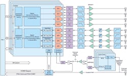
Separate phase-locked-loop (PLL) synthesizer ICs provide converter sample clock signals to each digitizing IC. Furthermore, a clock buffer IC supplies the digital reference and system reference clocks needed for multichip synchronization algorithms.1
The system is configured to operate within the S-band and sets the NCO frequencies such that the analog signal for all transmit and receive channels is the same at 2.7 GHz. Its digital-to-analog converter (DAC) sample rate is 12 GS/s, and the platform synthesizes transmit channels in the first DAC Nyquist zone. The analog-to-digital converter (ADC) sample rate is 4 GS/s, and the platform captures receive channels in the second ADC Nyquist zone.
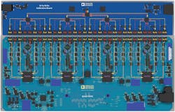
As shown in Figure 2, we used an attached 16-transmit/16-receive-channel calibration board to concisely loop back combined channel transmit signals into each receive channel. By doing so, we obtained a simultaneous capture of all receive channels. The system’s PLL synthesizers are then aligned using their own phase-adjustment blocks. Also, the transmit channels and receive channels are coarsely aligned using the NCO phase-offset blocks provided in the digital upconverters (DUCs) and digital downconverters (DDCs), respectively.
The end result is the subsystem being roughly phase-aligned at the calibration frequency as in the plot depicted in Figure 3 from Part 1, but no amplitude alignment is yet achieved. We’ve used the 16-transmit/16-receive-channel calibration board for purposes of this article to electrically align the system. However, a similar configuration could be obtained over the air with the use of system-calibration reflectors that also help to correct any antenna channel-to-channel anomalies.
As seen in Figure 1, 96-tap pFIR filters are located at the output of each ADC, such that the phase and amplitude response of each ADC channel can be aligned to the others throughout the frequency span of the full ADC sample rate. This places the pFIR filters between the ADCs and the DDC blocks. As such, the digital interface’s data rate is different from that of the pFIR rate, and so we must know the amount of frequency translation and rate decimation in the system to use the pFIRs for channel-amplitude alignment.
Because we’re sampling real data at the input of each ADC for this article, the pFIR inputs are real-valued. Moreover, the system design is configurable such that one pFIR block per ADC pair is the implemented solution, as shown by the dual real block in Figure 1. This alternatively allows the use of I/Q complex inputs into two separate ADCs to enable system alignment.
To amplitude-align and amplitude-flatten the channels in the system, we loaded a wideband chirp waveform into each transmit channel so that it encompasses all frequencies within the I/Q bandwidth of the system. Thus, the user can determine the frequency error response for all frequencies within the system’s data rate. Then, we obtained a baseline data capture at the decimated I/Q data rate.
Error Response Results
For the results in this article, we used an ADC sample rate of 4 GS/s and an I/Q data rate of 250 MS/s. As such, each transmit NCO frequency is set to 2.7 GHz and each receive NCO frequency is set to 1.3 GHz due to frequency folding from the second Nyquist zone down to the first Nyquist zone. We captured the baseline data using a MATLAB system interface, and calculated magnitude and phase error responses for each channel with respect to a gain-flattened Rx0, whereby the maximum value received for all receive channels is the ideal received input throughout the full I/Q band.
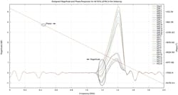
Figure 3 shows the phase and amplitude error responses of four of the 16 receive channels in the system. The left side of Figure 3 shows that the NCO phase offsets tend to mostly correct the phase errors of each receive channel. However, as can be observed from the right side of Figure 3, amplitude errors remain in the system. The remainder of the 12 receive channels have similar error responses.
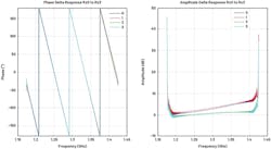
Also note that not only are the receive amplitudes not identical to Rx0, but there’s also poor amplitude flatness without the use of additional calibration techniques. These anomalies are intentionally introduced using analog filters in the ADC front-end networks to enable demonstration of amplitude flatness and equalization.
Designing pFIRs
Therefore, to improve amplitude alignment and amplitude flatness, real-valued, 96-tap arbitrary magnitude and phase pFIRs are designed based on the complex-valued error response of each channel with respect to the gain-flattened Rx0. Care is taken such that the pFIR design algorithm more heavily weighs the error response of the narrower I/Q band of interest. However, the full pFIR design covers the wider full-rate ADC Nyquist zone, and the regions outside of the 250-MHz sub-band are forced to a unity-passband response. Therefore, for this article, a sub-band of 250 MHz centered at the receive NCO frequency (1.3 GHz) is more heavily weighted for the pFIR design than the remainder of the Nyquist zone.
Though these pFIRs are designed using filter design functions within MATLAB’s DSP System Toolbox, similar algorithms can alternatively be used in hardened digital circuitry for fielded systems. Figure 4 shows the designed 96-tap pFIR filters for two of the 16 receive channels used in the example for this article. The pFIR design for the remaining 14 receive channels is similar.
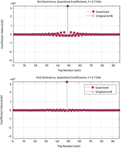
Figure 5 reveals the designed pFIR magnitude and phase response across the full Nyquist zone for all 16 receive channels in the subarray.
It’s important to note that pFIR design algorithms typically design over continuously valued coefficient space between a value of zero and one. However, hardware requires that these continuously valued coefficients be quantized and forced within a certain bit width available on the system. This system uses a varying bit width for the pFIR coefficient space such that some coefficients are 16 bits, others are 12 bits, and still others are only 6 bits.
In addition, the 12-bit coefficients must reside next to the 16-bit coefficients. As can be observed from the coefficient values in Figure 4, only the larger-valued coefficients require 16 bits, whereas the smaller-valued coefficients only require 6 bits. However, any time ideal filter coefficients are quantized, a quantization error is introduced. Care is taken to minimize such a quantization error for this article so that the designed coefficients still fit within the available coefficient space.
After performing quantization, the pFIR coefficients are loaded into each channel with the aid of application-programming-interface (API) functions provided with the digitizer IC. Serial peripheral interface (SPI) communication via the API was used to modify each channel’s coefficients. However, dedicated general-purpose input/output (GPIO) signals can alternatively be employed to switch between different coefficient banks more quickly if needed.
Finally, we obtained a subsequent receive data capture while the pFIRs are enabled to analyze the pFIR design’s effectiveness. The top row of plots in Figure 6 shows the results prior to enabling the pFIRs. Notice that prior to the amplitude-equalization steps, the 16 receive channels maintain varying amplitudes and phases across the frequencies of interest. Also note that eight receive channels have different amplitude-flatness responses than do the other eight.
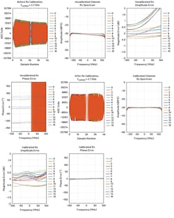
However, after designing and enabling the pFIRs for each receive channel, as can be observed from the bottom of Figure 6, the amplitudes of all receive channels are nominally amplitude-equalized, amplitude-flattened, and phase-aligned across the I/Q bandwidth. Additional amplitude and phase equalization improvements can be made with more refined pFIR designs, but that was beyond the scope of this article.
In the next part of this series, we will cover digitizing element resource consumption versus FPGA resource consumption, and then compare their power consumption.
Reference
1. Mixed-Signal and DSP Design Techniques, Digital Filters. Analog Devices, Inc.
About the Author
Mike Jones
Principal Electrical Design Engineer, Analog Devices Inc.
Mike Jones is a principal electrical design engineer with Analog Devices working in the Aerospace and Defense Business Unit in Greensboro, N.C. He joined Analog Devices in 2016. From 2007 to 2016 he worked at General Electric in Wilmington, N.C., as a microwave photonics design engineer working on microwave and optical solutions for the nuclear industry. He received his BSEE and BSCPE degrees from North Carolina State University in 2004 and his MSEE from North Carolina State University in 2006.
