Improving Wideband Multichannel Systems with IC Integration (Part 1)
Members can download this article in PDF format.
What you’ll learn:
- How greater silicon integration leads to reductions in power consumption and SWaP.
- Integrated DSP blocks serve as compensation filters for downstream elements.
- Digital up/downconverter blocks enable multiple digital channels within the converter’s instantaneous bandwidth.
Over the past several decades, channel counts and bandwidths in wireless systems have steadily increased. The driving factors for these modern telecommunication, radar, and instrumentation systems are their data rates and overall system-performance requirements. However, these requirements also have increased power envelopes and system complexities, making power density and component-level features more important.
To help address some of these limitations, the semiconductor industry has integrated more channels on the same silicon footprint, thereby reducing watt-per-channel requirements. In addition, semiconductor companies are integrating more complex features into digital front ends that ease the off-chip hardware design. These sorts of integrations have historically been achieved in an application-specific integrated circuit (ASIC) or field-programmable gate array (FPGA) fabric. Features can range from generic components like filters, downconverters, or numerically controlled oscillators (NCOs), to more complex application-specific operations.
Signal conditioning and calibration problems only become more compounded when developing high-channel-count systems. Such architectures may require unique filters or other digital-signal-processing (DSP) blocks per channel, thereby making the shift to hardened DSP more important for power savings.
This article, the first in a three-part series, presents experimental results utilizing a 16-channel transmit and 16-channel receive subarray in which all transmit and receive channels are calibrated using hardened DSP blocks within the digitizer integrated circuit (IC). The resulting multichannel system improves size, weight, and power (SWaP) performance when compared to other architectures. When comparing the resource utilization of an FPGA for the system, it becomes clear that the hardened DSP blocks solve significant challenges for designers of multichannel platforms.
DSP Blocks
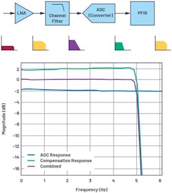
Real-world signals, whether used for synthesis or reception, require some amount of analysis or processing to collectively achieve the performance required for any application. A common method to compensate for signal-chain amplitude droop or flatness is to leverage compensation filters. Figure 1 shows an example of a gain and flatness compensation filter designed and used to correct imperfections across a given frequency band, thereby creating a more ideal response for downstream applications.
For multichannel systems, this processing must allow for independent control on a per-channel basis to isolate each channel’s performance with respect to another. Therefore, separate DSP blocks are utilized in this system to achieve channel phase and amplitude alignment while also attaining gain flattening within the passband of interest. Because each channel and system are unique, the DSP must be tuned specifically for that configuration, environment, and hardware lot.
Digital Up/Downconverter Blocks
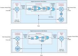
The results of this article hinge on heavy use of digital-upconverter (DUC) DSP blocks and digital-downconverter (DDC) DSP blocks collocated within monolithic DACs and ADCs. Figure 2 shows an example of a DUC and DDC block diagram revealing the details of these often-used data paths.
DUC and DDC blocks can serve many useful purposes:
- Interpolate (DUC) and decimate (DDC) the converter sample rate as compared to the digital interface’s data rate.
- Translate the frequency of the to-be-synthesized DAC data (DUC) and the digitized ADC data (DDC).
- Channelize the digital data transmitting on the interface to the baseband processor (BBP).
- Enable digital gain for each channel to generate code values closer to the system’s full-scale value.
- Enable injection of simple digital tones to ease system bring-up without the need for digital data links.
- Align the phases of each channel with respect to a common reference.
It’s often desired that the digital data rate offloaded to or from a converter be different than that of the converter’s sample rate. This can reduce system power consumption and improve overall system flexibility. Therefore, designers often implement digital upconverter and downconverter blocks.
DUC blocks allow the transmit waveform data from a BBP to be transmitted at a lower rate than the DAC’s sample rate, and thereby make it possible for interpolated waveform data to be synthesized by the DAC at this higher rate, as shown within the interpolation sub-block at the top of Figure 2. Similarly, DDC blocks allow the receive input to be digitized at a higher-speed ADC sample rate prior to being decimated and then sent to the BBP at a lower data rate, as shown within the decimation sub-block at the bottom of Figure 2.
Furthermore, frequency translation is often desired within the digital domain to synthesize or analyze higher-frequency analog signals when compared with those signals sent over the digital interface to or from the BBP. Many systems utilize complex-valued NCOs within DUCs and DDCs to achieve this frequency translation (Fig. 2, again).
NCOs can be regarded as digital signal generators. They may serve as a local oscillator (LO)-equivalent signal that, when sent into a digital mixer also contained within the DUC/DDCs, can increase the transmit waveform’s frequency sent into the DAC (as in the DUC case) or decrease the receive waveform’s frequency sent out of the ADC (as in the DDC case).
When digital frequency translation occurs, the output of these digital mixers inside a DDC often becomes a complex-valued signal. In this case, both in-phase (I) and quadrature-phase (Q) signals can propagate along a single digital channel ultimately attached to a sole ADC sampling real-valued data. Similarly, the input complex-valued signal to the digital mixer of the DUC’s digital gain block becomes real-valued at its output prior to being issued to a sole DAC synthesizing a real-valued signal.
Furthermore, DUCs and DDCs enable users to achieve multiple digital channels within the converter’s instantaneous bandwidth. Thus, more data streams are capable of being synthesized and/or analyzed by the BBP than the number of converters in the subarray itself. The result is a system that can provide improved signal synthesis or analysis for cases involving two narrow channels separated far apart.
Digital-Gain and Phase-Offset Blocks
As can be observed in Figure 2, digital gain blocks also are frequently present in DUCs and DDCs. The digital gain is enabled by providing a static digital code value to the input of another digital mixer in the sub-block. By using this feature, the user can achieve code values closer to the full-scale value provided by the number of bits utilized for the digital interface.
Similarly, dc offset continuous-wave (CW) tones can be injected instead of baseband data by simply providing a continuous static code value into one port of the digital mixer. This allows the user to easily synthesize transmit CW tones via the DAC into the analog domain without the need to establish JESD204B or JESD204C data links with the BBP.
Phase-offset blocks are often implemented at the output of the NCOs (Fig. 2, again). These phase offsets can be employed to correct channel-to-channel phase anomalies with respect to a common baseline reference present in the system. Because each DUC and DDC contains its own NCO, this makes it possible to achieve phase alignment for each channel in the system simply by offsetting the phase of the NCO by a determined amount for a given NCO frequency. The result, when used in conjunction with available multichip synchronization algorithms, is a deterministic phase relationship between all channels that can be corrected with these NCO phase offsets.1
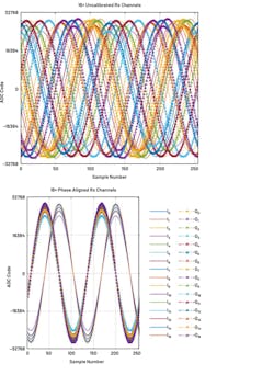
Figure 3 shows the experimental results of 16 simultaneous receive I/Q data captures before and after achieving phase alignment strictly by setting the required NCO phase offset values for each receive data path. Note that these digital corrections also correct the RF and microwave impairments located in the front-end networks for each channel.
In the next part of this article series, we’ll cover programmable finite-impulse-response (FIR) filters and how to achieve channel amplitude alignment and gain flattening.
Reference
1. Michael Jones, Michael Hennerich, and Peter Delos. “Power-Up Phase Determinism Using Multichip Synchronization Features in Integrated Wideband DACs and ADCs.” Analog Devices Inc., January 2021.
About the Author
Mike Jones
Principal Electrical Design Engineer, Analog Devices Inc.
Mike Jones is a principal electrical design engineer with Analog Devices working in the Aerospace and Defense Business Unit in Greensboro, N.C. He joined Analog Devices in 2016. From 2007 to 2016 he worked at General Electric in Wilmington, N.C., as a microwave photonics design engineer working on microwave and optical solutions for the nuclear industry. He received his BSEE and BSCPE degrees from North Carolina State University in 2004 and his MSEE from North Carolina State University in 2006.


