Platform Propels RF Designs from Concepts to Products
Download this article in PDF format.
Accelerating wireless communications and other electronic products driven by coming 5G networks, Internet of Things (IoT) applications, and ADAS vehicles are pressuring engineers to develop unique solutions more quickly and efficiently. As a result, RF/microwave designers must develop smaller, more capable antenna and other RF front-end components in less time than before.
In many cases, engineers must adapt novel designs based on evolving techniques and materials, advanced device integration, and greater exploration of the design space with unique topologies and architectures. Fortunately, computer-aided-design (CAD) software can help, especially when it’s the latest version—V14—of the NI AWR Design Environment from National Instruments AWR.
As demands increase for new RF front-end components with higher levels of performance, such as improved linearity and lower noise figure, designers must learn to juggle an often-conflicting set of design parameters. Circuit, system, and electromagnetic (EM) simulation must work seamlessly together along with design automation that helps engineers define and manage complex RF electronics, including chip, package, and board structures.
Simulation must accurately predict the response to standards-based signals, and the environment must help engineers create and organize simulation results to gain insight into component behavior. And these capabilities must integrate well with other design tools. These qualities are built into NI AWR Design Environment software, inclusive of Microwave Office, Analog Office, Visual System Simulator (VSS), AXIEM, and Analyst software, providing a robust and complete platform for RF/microwave engineers to develop these next-generation communication electronics.
The V14 release of NI AWR Design Environment software focuses on all of these stages of RF/microwave design. It emphasizes accelerating design starts through powerful network synthesis, enhanced design flow automation for printed-circuit-board (PCB) and module design, phased-array antenna system generation, and standards-compliant test benches. In addition, solver improvements provide fast and reliable simulation, as well as tuning and optimization, to help engineers convert their initial design starts into physically realizable RF components and systems. Powerful data visualization through dynamic data reporting and linked measurements provides a better understanding of how design choices impact performance. On top of that, enhanced automation within NI AWR software further supports back-end design operations.
Aiding Design Flow
Design-flow automation connects simulation models, third-party tools, and layout geometries to printed circuit board (PCB), monolithic microwave integrated circuit (MMIC), RFIC, and multichip module manufacturing processes. This expedites EM verification of passive structures and board/package designs and enables the extracted models to be incorporated into circuit- or system-level analysis. The V14 release of the NI AWR Design Environment features new functionality that assists users with design starts, design entry, analysis/optimization, and report generation. Such capabilities allow users to manage measurement data sources and parameters from a single location and create sets of linked reports in a single dashboard display.
When pursuing a complex set of component performance specifications, designers often must simultaneously track multiple simulation results. In support of this, V14 of the NI AWR Design Environment enables users to manage measurement data sources and parameters from a single location. Thus, they can create sets of linked reports in a single dashboard display. Variables can be used to define and control groups of measurement parameters together.
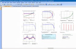
1. The dynamic data display in the V14 release of the NI AWR Design Environment automatically updates graphs, while the accompanying embedded window provides a great deal of user control and flexibility in analyzing and showing results.
Users are able to combine measurement variables, document sets that create a symbolic link of one or more simulation documents that can be used by measurements, and embedded plots within a new window-in-windows feature coupled with an output equation document. This document helps create a dynamic data display that automatically updates graphs and embedded windows with the single click of a computer mouse. For power-amplifier (PA) designers, these new capabilities make it possible to directly plot measurements versus output power (or voltage or current) and/or define the output power measurement on the schematic more easily (Fig. 1).
Phased Arrays
The newly enhanced phased-array generator wizard lets users interactively design phased-array antenna systems and then generate schematics or system diagrams representing designs in formats most suitable for further analysis. This latest version of the software suite makes it possible to easily define a phased-array geometry (configuration), feed structures, gain tapers, and the characteristics of individual array elements and their respective RF links.
When performing a simulation, the array response is immediately displayed and reflects any changes due to the operating signal power level, beamsteering, or element failures. Once the design is complete, the phased-array generator wizard produces a system diagram implementation that can be further analyzed in VSS software or be incorporated as part of a larger, complete VSS communication system.
Another role of the phased-array generator wizard is to create schematics/layouts for full EM analysis with the software suite’s AXIEM planar EM simulator or Analyst finite-element-method (FEM) three-dimensional (3D) simulator. It also creates schematics/layouts by performing analysis with third-party EM tools such as the ANSYS High-Frequency Structure Simulator (HFSS) software.
Preparing for 5G
Multiple-in, multiple-out (MIMO) and beamsteering phased-array antennas are enabling technologies for achieving the over-the-air spatial efficiency called for by 5G and emerging radar applications such as self-driving cars. In addition to the enhanced phased-array generator wizard, new standards-compliant WINNER II and 5G spatial channel models are available as an add on-module. This module provides high-accuracy modeling of channel-specific propagation effects that support more realistic link-budget analysis for rapid validation of end-to-end system performance and specification of individual component requirements.
The updated VSS model library offers data encoding/decoding and signal generation/analysis for the latest 5G New Radio (NR) specifications. With new VSS projects that support LTE, 5G transmit (TX) and receive (RX), and narrowband IoT (NB-IoT) standards-compliant signals and test benches, engineers can simulate systems or perform measurements on components based on the corresponding specifications.
VSS V14 supports an NB-IoT uplink coexistence RX test bench, an NB-IoT uplink enriched narrowband (eNB) RX test bench in the guard band of an LTE signal, and an in-band uplink eNB RX test bench. Component designers and system architects can use the default configurations to perform what-if analyses or modify them as needed. It also adds new data encoding and decoding capabilities for LTE, NR, and DVB-S2, including support for various low-density parity check (LDPC) codes.
Network Synthesis Wizard
The new network synthesis wizard is an add-on utility for creating optimized two-port impedance-matching networks of discrete and distributed components. To create an impedance-matching network, a user specifies the maximum number of sections and the types of components to include in the search space. Using the evolutionary algorithms employed within AntSyn antenna design and synthesis software, the network synthesis wizard searches for the best circuit typologies and optimizes the component parameter values.
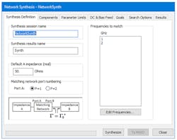
The user interface for the network synthesis wizard lets designers interactively develop an unlimited number of networks optimized for noise, power, or impedance matching between amplifier stages or different components, such as an amplifier and an antenna. The optimum reflection coefficients are found for specified frequencies and can be provided in the form of load-pull data, network-parameter data files, or circuit schematic diagrams. On the synthesis definition tab, users can specify a default impedance or the impedance of the desired source/load network, as well as the desired match frequencies (Fig. 2).
2. The network synthesis wizard guides designers through the development of inter-component and amplifier impedance matching for specific frequencies.
The NI AWR Design Environment V14 release offers significant new functionality to help guide designers developing circuit-level components—from generating circuit topologies that achieve specified performance goals to interactively optimizing element parameter values to improve overall circuit behavior. The new tuner interface utilizes space-efficient horizontal sliders to support parametric tuning of complex designs with many variable design properties, while the updated property dialog provides greater control and organization of element parameters.
Faster EM
The AXIEM and Analyst EM simulators apply Maxwell’s equations to compute the electrical behavior of a structure from its physical geometry. The AXIEM simulator provides responses for 3D planar structures such as transmission lines, spiral inductors, and metal-insulator-metal (MIM) capacitors, whereas the Analyst simulator addresses arbitrarily shaped 3D objects such as wire bonds, ball grids, finite substrates, and 3D horn antennas.
Multiple V14 software improvements target EM analysis and supporting design flows, delivering enhanced layout editing, new EM-port types and faster, more powerful solver technology. Additionally, the new planar body wrapping feature supports modeling and EM analysis of conformal structures such as embedded antennas found in consumer electronics and mobile and IoT devices.
Novel port technology helps design engineers characterize substrates more effectively. 3D EM internal wave ports support characterization of complex MMIC and RFIC structures with excitation ports that are not located on a defined simulation boundary. For PCB modeling, new features support port points that allow exact placement of surface-mount components, frequency-dependent materials, and the ability to solve inside metal structures, providing users with greater accuracy.
New functionality added to the PCB import wizard accelerates EM verification of designs created in board-layout tools from leading CAD vendors such as Cadence, Zuken, and Mentor Graphics with powerful geometry selection and editing capabilities. RF design engineers can easily isolate areas of interest with powerful net and area selection for faster, more reliable EM analysis and optimization. It’s possible to extract broadband S-parameters for critical traces and densely populated circuit boards, where unintended coupling and parasitic elements can be detected and addressed before they cause design failures.
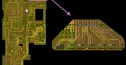
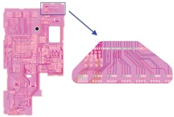
3. Versatile editing capabilities in the V14 release of the NI AWR Design Environment work with AXIEM and Analyst simulators to speed the design of high-frequency circuits and modules.
The powerful new editing capabilities within the NI AWR Design Environment V14 release enable RF designers to easily set up complex imported PCB designs for analysis in the AXIEM or Analyst simulators. A new smart editing tool lets users interactively isolate circuit-board sections and multilayer traces and viaholes, automatically define unlimited EM ports from the imported data, generate an EM structure with schematic view for surface-mount component insertion, and perform related simulation setup tasks (Fig. 3). Finally, the enhanced iNet intelligent net functionality with improved trace routing addresses the need for rapid EM modeling and analysis of advanced modules, MMICs, and PCBs utilizing heterogeneous structures and dense networks of high-frequency interconnects.
The release of the V14 NI AWR Design Environment platform offers new and enhanced innovative solutions in design automation and simulation technology for the advancement of high-frequency electronic products serving communications and aerospace/defense industries. As component requirements for these applications drive advances in semiconductor, PCB, and multichip module integration, this latest NI AWR software addresses evolving product-development challenges with powerful enhancements in design flow automation and greater speed and accuracy for its system, circuit, and EM simulation technologies.
National Instruments, AWR Corp., 1960 E. Grand Ave., Ste. 430, El Segundo, CA 90245; (310) 726-3000, FAX: (310) 726-3005.
About the Author
David Vye
Technical Marketing Director, Cadence
David Vye is the senior product marketing manager for AWR software at Cadence, where he’s responsible for product messaging and positioning in the RF/microwave market. A former editor and business development manager for Microwave Journal, David has held a number of technical and marketing positions throughout the RF/microwave industry. He holds a BSEE from the University of Massachusetts at Dartmouth, with a concentration in microwave engineering.
Jack Browne
Technical Contributor
Jack Browne, Technical Contributor, has worked in technical publishing for over 30 years. He managed the content and production of three technical journals while at the American Institute of Physics, including Medical Physics and the Journal of Vacuum Science & Technology. He has been a Publisher and Editor for Penton Media, started the firm’s Wireless Symposium & Exhibition trade show in 1993, and currently serves as Technical Contributor for that company's Microwaves & RF magazine. Browne, who holds a BS in Mathematics from City College of New York and BA degrees in English and Philosophy from Fordham University, is a member of the IEEE.


