Dealing with Differences in RF Semiconductors
Download this article in PDF format.
Selecting semiconductors for RF/microwave applications involves choosing from among a large array of devices fabricated on different substrates. As the industry hopes to combat the ever-increasing congestion of lower-frequency spectrum with signal bandwidths reaching into the millimeter-wave (mmWave) range, semiconductor materials and devices will be pushed into new regions to achieve more gain and power at higher frequencies.
Bipolar junction transistors (BJTs) fabricated on silicon (Si) substrate wafers—the oldest transistors used in microwave circuits—are still used in both low- and high-power applications. Si bipolar transistors are simple devices that can operate with a single positive voltage supply but provide reasonable gain through RF and lower microwave frequencies.
As with many other high-frequency transistor configurations, BJTs consist of several semiconductor diode junctions, fabricated from layers of p-type and n-type semiconductor materials. The p and the n refer to “positive” and “negative” and denote whether a material has an excess of holes or electrons, respectively. They also indicate how the current will flow in a semiconductor device formed of the materials.
A BJT has three terminals—the base, collector, and emitter—with the voltage between two of the terminals, such as the base and the emitter, serving to control the flow of current from the other terminal, such as the emitter. The input current to a Si BJT controls the flow of output current. Si BJTs can be fabricated as pnp devices, with an n-type semiconductor layer between two p-type layers, or as npn devices, with a p-type semiconductor layer between two high-electron-content n-type layers.
Si has been a long-running starting point for many different types of high-frequency transistors, including the Si metal-oxide semiconductor field-effect transistor (MOSFET) and Si laterally diffused MOS (LDMOS) transistors. In a Si MOSFET, the three terminals are called the gate, source, and drain. Whereas the gain of a BJT does not fluctuate with bias voltage, the gain of a Si FET can vary with changes in input voltage, which typically results in Si BJTs providing better linearity than Si FETs for a given set of operating conditions.
While major suppliers have supported the different types of FETs based on Si substrates, alternative substrate materials, such as silicon carbide (SiC), are also used to fabricate MOSFET devices with the goal of achieving higher-power-handling capabilities. Cree Inc. and its Wolfspeed power and RF division have developed product lines of high-power, high-voltage MOSFET devices on SiC according to the various benefits of the semiconductor material: high breakdown voltage, higher thermal conductivity than Si, and wider bandgap (for higher voltage and higher power) than Si MOSFETs.
The usable gain of Si-based semiconductors, whether BJTs or FETs, is usually defined by a device’s transition frequency (fT), the point at which the gain drops to unity. For usable gain in a practical amplifier, the high-frequency limit will be considerably less than fT, though. Still, fT is a device performance parameter that can be useful when sorting through different discrete or even IC devices when seeking semiconductors for high-frequency amplifiers and other applications.
Si-based transistors with fT’s of 20 GHz or higher are not unusual, although a circuit with such a device at that frequency will function more as a conductor than an amplifier due to unity gain. The actual upper-frequency limit for a practical power amplifier (PA) or low-noise amplifier (LNA) with a 20-GHz fT might be more like one-tenth of that frequency, or about 2 GHz where there’s still usable gain.
Compound Semiconductors
Since the gain of Si BJTs and different types of MOSFETs drops at higher frequencies, over time semiconductor device developers have looked to other substrate materials, notably those with higher electron mobilities to support higher-speed, higher-frequency devices. Compound semiconducting materials having covalent bonds with eight electrons consist of materials with three and five valance electrons. For example, gallium with three valance electrons and arsenic with five valence electrons forms gallium arsenide (GaAs), or gallium and nitrogen (with five valence electrons) forms gallium nitride (GaN).
The high electron mobilities of these semiconductor materials has enabled the fabrication of high-power transistors into the microwave and mmWave frequency ranges. It’s also opened the door to small-signal, low-noise transistors well into the mmWave frequency range, to about 150 GHz, for low-noise satellite receivers and other communications radio applications.
GaAs and GaN III-V compound semiconductor materials, as they are known, are typically combined with other compound materials, such as SiC and aluminum-GaAs (AlGaAs), to improve thermal management of the heat produced by the inefficiencies of different transistor and amplifier architectures (see "Striking the Right Balance: RF Power Output and Efficiency"). Additional semiconductor substrate materials, such as indium phosphide (InP) and silicon germanium (SiGe), have also been used in attempts to fabricate transistors capable of gain at extremely high mmWave frequencies.
Metal-epitaxial-semiconductor field-effect transistors (MESFETs) fabricated on GaAs semiconductor wafers have for decades served both large-signal and small-signal (low-noise) markets in commercial and military applications through microwave frequencies, in both discrete-transistor and monolithic-microwave-integrated-circuit (MMIC) forms. More recently, high-electron-mobility transistors (HEMTs) fabricated on GaN base materials, often with SiC or AlGaAs, have shown some of the capabilities of high-power-density substrate materials like GaN and SiC in the creation of power transistors at microwave frequencies.
Surveying Examples
What kinds of RF/microwave power levels are available from commercial discrete transistors fabricated on the different semiconductor materials and using different device architectures? The simplest answers are that silicon-based devices are capable of very high output power levels but at lower frequencies, while GaAs and GaN transistors may be limited in output power compared to silicon transistors but are usable at much higher frequencies.
Various transistor architectures have evolved over time in attempts to optimize the different semiconductor materials for maximum gain, frequency, and/or output power, such as heterojunction bipolar transistors (HBTs), HEMTs, and LDMOS devices. However, each transistor is different and offers its own set of performance levels to evaluate, with many tradeoffs to consider especially in terms of gain, output power, and frequency.
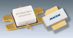
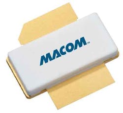
Silicon bipolar transistors are still used for many RF pulsed and CW applications, largely below 1 GHz, with output-power capabilities depending on frequency and bandwidth. For example, the model MRF10350 Si bipolar transistor from MACOM is designed for pulsed PAs, such as in Mode-S aviation radar transmitters from 1025 to 1150 MHz. The silicon-nitride-passivated device, which features a gold-metallized emitter, comes in a hermetic metal flange package (Fig. 1) to handle excess heat from high power levels. It’s rated for 350 W peak output power when amplifying microsecond-length pulses, and provides at least 8.5-dB gain with 40% efficiency at +50-V dc bias.
1. This hermetic package holds a high-power, +50-V dc Si bipolar transistor capable of 350 W pulsed output power from 1025 to 1150 MHz for Mode-S aviation radar transmitters. (Courtesy of MACOM)
At slightly higher frequencies, the model AFV141KH enhancement-mode Si LDMOS transistor from NXP Semiconductors (www.nxp.com) targets pulsed L-band amplification applications from 1200 to 1400 MHz. It runs on a +50-V dc supply and provides as much as 1000 W output power and 16-dB gain with 300-µs pulses at 12% duty cycle. The LDMOS transistor is supplied in a ceramic flange-mount package.
From the same supplier, but with added integration, the model AFIC31025N is a Si LDMOS device that can be considered a PA; it consists of several transistor stages with impedance matching to 50 Ω. The output contributions of individual LDMOS devices are combined to achieve higher output power levels within a transistor package.
The AFIC31025N operates at S-band from 2.4 to 3.1 GHz and can be used for both CW and pulsed signals. It provides 25 W CW output power from 2.4 to 2.5 GHz with 30-dB power gain. At higher frequencies, it also delivers 25 W output power, from 2.7 to 3.1 GHz, but with 22-dB power gain for 200-µs pulses at 15% duty cycle. It’s designed for maximum operating voltage of +32 V dc and is a good fit for S-band civilian, weather, and maritime radar transmitters. It’s supplied in a plastic flange-mount package.
GaAs power transistors are often housed as internally matched devices to optimize output power, such as the model TIM1314-30L from Toshiba Corp. Supplied in a flange-mount hermetic package, it supplies +45 dBm (32 W) output power at 1-dB compression from 13.75 to 14.50 with 5-dB gain. Designed for +10-V dc operation, it maintains gain flat flatness of ±0.8 dB or better across its bandwidth, with PAE of typically 22%.
Of course, GaAs transistors may more commonly be found in LNAs, such as the model MGF4964BL from Mitsubishi Electric Corp., which is a GaAs HEMT that’s usable to about 25 GHz. It’s housed in a plastic Micro-X package since it offers negligible output power. Where it excels is at the receive side of systems, with a typical noise figure of a mere 0.65 dB at 20 GHz, and associated gain of 13.5 dB at 20 GHz.
Going with GaN
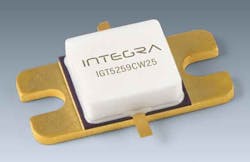
Integra Technologies, which offers an extensive line of Si LDMOS discrete and integrated devices, has developed packaged transistors based on GaN-on-SiC substrates for higher-frequency operation. One example is the IGT5259CW25 (Fig. 2), which delivers 25 W CW output power from 5.2 to 5.9 GHz with 12-dB power gain. It provides 48% typical efficiency when operating from a +36-V dc supply and within-package matching to 50 Ω. It can also be used in pulsed applications and provides 50 W output power and 14-dB gain when handling 1-ms pulses at 15% duty cycle and 80 W output power and 13-dB gain with 300-µs pulses at 10% duty cycle.
2. Housed in this package is a GaN-on-SiC discrete +36-V dc transistor capable of 25 W CW output power from 5.2 to 5.9 GHz with 12-dB power gain. (Courtesy of Integra Technologies)
The company also demonstrates what GaN-on-SiC transistors can do at higher frequencies with its model IGT1112M90, which is rated for 90 W peak output power from 11 to 12 GHz. It achieves somewhat lower efficiency at these higher frequencies, at typically 37%, but still provides 9-dB power gain for 150-µs pulses at 10% duty cycle
Curiously, Integra offers both Si LDMOS and GaN on SiC packaged transistors for the same frequencies and operating conditions (same applications), allowing customers to specify their technology of choice between two very similar transistor devices. As Chris DeMartino explains here, GaN has benefits at higher frequencies, but when Si, GaN, and even GaAs devices are compared under similar conditions and device architectures, there’s often very little separating the semiconductor materials.
Both the Si LDMOS model ILT2731M and the GaN/SiC IGT2731M130 from Integra are designed for pulsed use from 2.7 to 3.1 GHz. When characterized with 300-µs pulses at 10% duty cycle across that 400-MHz bandwidth, each device delivers 130 W peak output power, although with differences in gain and efficiency. The Si LDMOS device provides 12-dB gain and 43% PAE when operating from a 32-V dc supply, while the GaN/SiC device delivers 15-dB gain with 50% from a higher-voltage +50-V dc supply. If anything, for two devices optimized for the same 2.7-to-3.1-GHz range, the comparison shows the higher-energy, higher-frequency potential of GaN semiconductor materials.
For those interested in the latest developments in wide-bandgap semiconductor technology, the Power Sources Manufacturers Association (PSMA) Semiconductor Committee is sponsoring three industry sessions at APEC 2019 (March 19-21, 2019, Anaheim Convention Center). The sessions explore the rapid emergence of wide-bandgap semiconductors as a significant power-conversion technology. The sessions cover switching and high-power generation for wide-bandgap devices, including GaN and SiC power semiconductors.
About the Author
Jack Browne
Technical Contributor
Jack Browne, Technical Contributor, has worked in technical publishing for over 30 years. He managed the content and production of three technical journals while at the American Institute of Physics, including Medical Physics and the Journal of Vacuum Science & Technology. He has been a Publisher and Editor for Penton Media, started the firm’s Wireless Symposium & Exhibition trade show in 1993, and currently serves as Technical Contributor for that company's Microwaves & RF magazine. Browne, who holds a BS in Mathematics from City College of New York and BA degrees in English and Philosophy from Fordham University, is a member of the IEEE.


