Download this article in PDF format.
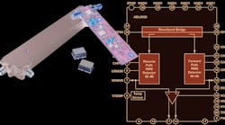
Directional couplers are used in a wide variety of applications to sense RF power, and they may appear at multiple points in a signal chain. In this article, we will explore Analog Devices’ ADL5920, which combines a broadband directional bridge-based coupler with two rms responding detectors in a 5- × 5-mm surface-mount package. This device helps overcome the struggle that conventional discrete directional couplers deal with regarding the tradeoff between size and bandwidth, particularly at frequencies below 1 GHz.
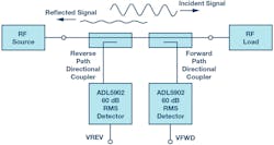
In-line RF power and return loss measurements are typically implemented using directional couplers and RF power detectors. In Figure 1, a bidirectional coupler is used in a radio or test-and-measurement application to monitor transmitted and reflected RF power. It’s also sometimes desirable to have RF power monitoring embedded in a circuit, with a good example being where two or more sources are being switched into the transmit path (either using an RF switch or with external cables).
1. Measuring forward and reflected power in an RF signal chain.
Directional couplers have the valuable characteristic of directivity—that is, the ability to distinguish between incident and reflected RF power. As the incident RF signal travels through the forward path coupler on its way to the load (Fig. 2), a small proportion of the RF power (usually a signal that’s 10 to 20 dB lower than the incident signal) is coupled away and drives an RF detector. Where both forward and reflected power are being measured, a second coupler with reverse orientation compared to the forward path coupler is used. The output-voltage signals from the two detectors will be proportional to the forward and reverse RF power levels.
2. A typical RF power measurement system using directional couplers and RF detectors.
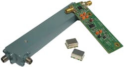
Surface-mount directional couplers suffer from a fundamental tradeoff between bandwidth and size. While bidirectional directional couplers with one octave of frequency coverage (that is, FMAX is equal to twice FMIN) are commonly available in packages as small as 6 mm2, a multi-octave surface-mount directional coupler will be much larger (Fig. 3). Broadband connectorized directional couplers have multi-octave frequency coverage, but they’re significantly larger than surface-mount devices.
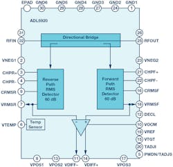
Figure 3 also shows the evaluation board for the ADL5920, a new RF power detection subsystem with up to 60 dB of detection range, housed in a 5- × 5-mm MLF package (the ADL5920 IC is located between the RF connectors). The block diagram for the ADL5920 is shown in Figure 4.
3. Connectorized directional coupler, surface-mount directional coupler, and ADL5920 integrated IC with directional bridge and dual rms detectors.
4. Shown is a block diagram of the ADL5920.
Instead of sensing the forward and reflected signals using directional couplers, the ADL5920 uses a patented directional bridge technology to achieve broadband and compact on-chip signal coupling. To understand how a directional bridge works, we need to first take a step back and look at the Wheatstone bridge.
Wheatstone Bridge
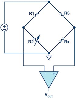
The notion of a directional bridge is based on the Wheatstone bridge (Fig. 5) that creates zero differential voltage when balanced. In a Wheatstone bridge, one resistor in one of the two legs is variable (R2), while two others (R1 and R3) are fixed. There are four resistors in total—R1, R2, R3, and Rx—where Rx is an unknown resistance. If R1 = R3, then when R2 is equal to Rx, VOUT = 0 V.
5. A Wheatstone bridge creates zero differential voltage when balanced.
The bridge is considered balanced when the variable resistor is of the correct value such that the voltage divide ratios on the left and right side of the bridge are equal. This creates a zero-volt differential signal across the differential sense nodes that produce VOUT.
A Unidirectional Bridge
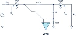
Figure 6 shows the schematic of a unidirectional bridge and it best explains the basic operation of such a device. First, it’s important to observe that a directional bridge needs to be designed for a particular Z0and that insertion loss is minimized. If RS = RL = R = 50 Ω, then the sense resistor of the bridge is 5 Ω, which is a good compromise between insertion loss (<1 dB) and signal sensing.6. Simplified unidirectional bridge diagram.
Calculating ROUT as seen looking back from the load results in an exact 50-Ω port impedance, while calculating RIN will result in 50.8-Ω port impedance (|Γ| = 0.008; RL = –42 dB; VSWR = 1.016). If a signal is applied as shown at RFIP then, since RIN ~50 Ω, the voltage at RFIP is about half of the source voltage. If we assume for a moment that the voltage at RFIP equals 1 V, then the voltage at RFOP will be about 0.902 V.
This voltage is further attenuated by 10/11 = 0.909 such that the negative input of the differencing amplifier is 0.82 V with a resultant differential voltage of (1 – 0.82) = 0.18 V. The effective forward coupling factor (Cpl) of this bridge is:
Balanced in the context of the bridge means that when a signal is applied in the reverse direction (RFOP to RFIP), then the VFWD detector (or Cpl port) will ideally see zero differential voltage, while it sees a maximum signal when the signal is applied in the forward direction (RFIP to RFOP). To get maximum directivity in such a structure, precision resistors are of utmost importance and that’s why integrating them is beneficial.
In a unidirectional bridge, to determine isolation, which is needed to calculate return loss, one needs to flip the device and then apply the input signal to RFOP. In that case, the bridge is balanced and the plus and minus inputs to the differential amplifier are equal, since the same divide ratios of 0.909 = (10R/(10R + R) = (R/(R+0.1R)) result in a differential voltage of (V+ minus V–) = 0 V.
A Bidirectional Bridge
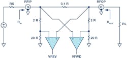
The bidirectional bridge in Figure 7 is similar to the one used in the ADL5920. The unit resistance R is equal to 50 Ω for a 50-Ω environment. So the value of the bridge’s sense resistor is 5 Ω, while the two shunt networks are each about 1.1 kΩ. This is a symmetric network, so the input and output resistances, RIN and ROUT, are the same and close to 50 Ω when RS and RL are also equal to 50 Ω.
7. Simplified bidirectional bridge diagram.
When the source and load impedance are both 50 Ω, an ohmic analysis of the internal network tells us that VFWD will be quite large compared to VREV. In a real-world application, this corresponds to maximum power transmission from source to load. This results in reflected power that’s small, which in turn leads to a very small VREV.
Next, let’s consider what happens if RL is either infinite (open circuit) or zero (shorted load). In both cases, if we repeat the ohmic analysis, we find that VFWD and VREV are approximately equal. This mirrors a real-world system where an open or shorted load results in forward and reflected power being equal. What follows is a more detailed analysis of these scenarios.
VSWR and Reflection Coefficient
A full analysis of errors in network analysis is too complicated and beyond the scope of this article, yet we want to summarize some of the basic concepts here. An excellent resource is the application note by Marki Microwave’s application note Directivity and VSWR Measurements.1
Traveling waves are important concepts to describe the voltages and currents along transmission lines since they are functions of position and time. The general solution of voltages and currents along transmission lines consist of a forward traveling wave and a reverse traveling wave, which are functions of distance x.2
In the equations above, V+(x) represents the voltage wave traveling toward the load, while V–(x) represents the voltage wave reflected from the load due to mismatch, and Z0 is the characteristic impedance of the transmission line. In a lossless transmission line, Z0 is defined by the classic equation:
The most common Z0 is 50 Ω for transmission lines. If such a line is terminated with its characteristic impedance, then it appears to a 50-Ω source as an infinite line. That’s because any voltage wave traveling down the line will not result in any reflections that can be sensed at the source or anywhere else along the line. However, if the load is different from 50 Ω, then a standing wave will be generated along the line that can be detected and is defined by the voltage standing wave ratio (VSWR).
More generally, the reflection coefficient is defined as:
where Γ0 is the load reflection coefficient and γ the propagation constant of the transmission line.
R, L, G, and C are the resistance, inductance, conductance, and capacitance per unit length of the transmission line.
The return loss (RL) is the negative of the reflection coefficient (Γ) in dB. This is important to point out as reflection coefficient and return loss are frequently confused and used interchangeably.
Another very important definition of return loss in addition to the load mismatch above is in terms of incident and reflected power at an impedance discontinuity. This is given by:
and extensively used in antenna design. VSWR, RL, and Γ0 are related as follows:
Equation 14 and Equation 15 represent the maximum and minimum of the standing wave voltages. VSWR is defined as the ratio of the maximum to the minimum voltage along the wave. The peak and minimum voltages along the line are:
For example, in a 50-Ω transmission line, if the forward traveling voltage signal has a peak amplitude of A = 1 and the line is matched with a perfect load, then |Γ0| = 0, there’s no standing wave (VSWR = 1.00), and the peak voltage along the line is A = 1. However, if RLOAD is 100 Ω or 25 Ω, then |Γ0| = 0.333, RL = 9.542 dB, and VSWR = 2.00, with |V(x)|max = 1.333 and |V(x)|min = 0.666.
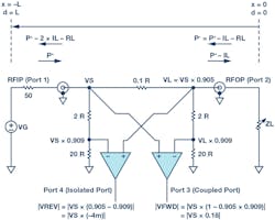
Figure 8 is a replica of Figure 7, but with signals shown in the default forward configuration and with traveling power waves indicated where the reference plane is at the load. At low frequencies where the wavelength is long relative to the physical structure, voltages and currents are in phase and the circuit can be analyzed according to Ohm’s law.
8. Simplified bidirectional bridge with signals.
The ports are defined as shown with the input port (Port 1) at RFIP, output port (Port 2) at RFOP, coupled port (Port 3) at VFWD, and isolated port (Port 4) at VREV. Since the structure is symmetric, the ports are reversed when a signal is reflected at ZL or applied to RFOP.
In the case of a matched load, and the generator voltage connected to Port 1 (RFIP), and with ZS = ZL = Z0 = R = 50 Ω:
and VL/VS+ is the insertion loss, LI, or IL in dB:
The attenuation factor for the two shunt legs on either side of the main line resistor of 0.1 × R is:
The equations in Figure 8 for |VREV| and |VFWD| show the values for those voltages with a signal applied in the forward direction. These equations indicate a fundamental directivity limit for the simplified schematic due to nonideal rejection at the isolated port of 33 dB:
From Figure 8, one can see that the directivity of the bidirectional bridge in the linear domain is determined by (Equation 21):
which shows that to increase directivity, α needs to equal the insertion loss, LI.
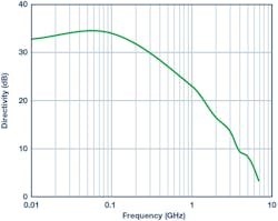
In silicon, the peak directivity is typically better than the simplified diagram would indicate (Fig. 9).
9. ADL5920 directivity vs. frequency—the input level is 20 dBm.
If ZL isn’t equal to Z0, as is normally the case, the coupled and isolated port voltages, which are complex, would be (Equations 22 and 23):
where VS+ is the forward voltage at Port 1 (node VS) and VL– is the reflected voltage from the load at Port 2 (node VL). Θ is the unknown phase of the reflected signal:
Substituting the equation above for VL– in Equations 22 and 23 (see notation above) and using Equation 21 (see notation above) to simplify the result, plus the fact that:
results in complex output voltages:
From these two equations, we can observe that for DL>>1 (Equation 28):
In the ADL5920, the voltages VREV and VFWD are mapped via two 60-dB range linear-in-dB rms detectors into voltages VRMSR and VRMSF that are (VISO/VSLP) and (VCPL/VSLP) in dB, respectively. Therefore, the differential output of the device VDIFF in dB represents (Equation 29):
where VSLP, the detector slope, is about 60 mV/dB.
Using the voltage-to-dB mapping of Equation 29 above in Equation 28 (see notation above):
And using Equation 9 (see notation earlier in article) in the equation above results in:
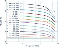
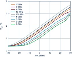
Figure 10 shows the response of the forward-power-sensing rms detector when the ADL5920 is driven in the forward direction. Each trace corresponds to the output voltage vs. frequency for a particular power level applied. While the plot stops at 10 MHz, operation at frequencies down to 9 kHz has been verified. In Figure 11, the same data is presented as output voltage vs. input power with each trace representing a different frequency.
10. Typical output voltage vs. frequency from the forward-path detector at multiple input power levels.
11. Typical output voltage vs. input power from the forward-path detector at multiple frequencies.
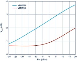
When the ADL5920’s RFOUT pin is terminated with a 50-Ω resistor, there should be no reflected signal. Therefore, the reverse-path detector should not register any detected reverse power. However, because the directivity of the circuit is nonideal and rolls off vs. frequency, some signal will be detected in the reverse path. Figure 12 shows the voltage measured on the forward- and reverse-path detectors at 500 MHz when RFIN is swept and RFOUT is terminated with 50 Ω. The vertical separation between these traces relates directly to the directivity of the bridge.
12. VRMSF and VRMSR output voltage vs. input power at 500 MHz when the bridge is driven from RFIN and RFOUT is terminated with 50 Ω.
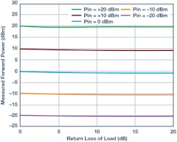
Figure 13 shows the effect of varying the load on the measurement of forward power. Defined power levels are applied to the RFIN input and the return loss of the load on RFOUT is varied from 0 to 20 dB. As expected, when the return loss is in the 10- to 20-dB range, the power-measurement accuracy is quite good. But as the return loss is reduced below 10 dB, the power-measurement error starts to increase. It’s notable that for a return loss of 0 dB, the error is still only in the 1-dB range.
13. Measured forward power vs. applied power and return loss of load, measured at 1 GHz.
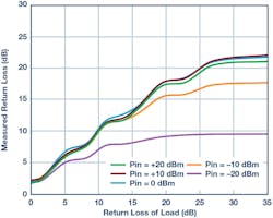
In Figure 14, the ADL5920 is being used to measure the return loss of the load, also at 1 GHz. A known return loss is applied to the RFOUT port. VRMSF and VRMSR are measured and the return loss is back-calculated.
14. Measured return loss vs. applied return loss and RF power, measured at 1 GHz.
There are a number of points to note about this plot. Firstly, it can be seen that the ADL5920’s ability to measure return loss degrades as the return loss improves. This is due to the directivity of the device. Secondly, note how the measurement accuracy degrades as the drive power drops. This is due to the limited detection range and sensitivity of the ADL5920 on-board rms detectors. The third observation relates to the apparent ripple in the traces. This is caused by the fact that each measurement is being taken at a single return-loss phase. If the measurement was repeated at all return-loss phases, a family of curves would result whose vertical width would be roughly equal to the vertical width of the ripple.
Applications
With the ability to measure inline RF power and return loss, the ADL5920 is useful for multiple applications. Its small size means that it can be dropped into many circuits without having a significant space impact. Typical applications include in-circuit RF power monitoring at RF power levels up to 30 dBm, where insertion loss isn’t critical. The return-loss measurement capability is typically used in applications where an RF load is being monitored. This could be a simple circuit to check that an antenna hasn’t been damaged or broken off (that is, catastrophic failure). However, ADL5920 can also be used to measure scalar return loss in materials analysis applications. This is most applicable at frequencies below approximately 2.5 GHz, where the directivity (and thereby the measurement accuracy) is greater than 15 dB.
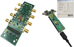
The ADL5920 is available to evaluate in two form factors (Fig. 15). The left side shows the traditional evaluation board where the detector output voltages are available on clip leads and SMA connectors. This evaluation board also includes a calibration path that can be used to calibrate out the insertion loss of the FR4 board.
15. Evaluation board options are available for the ADL5920.
The right side shows a more integrated evaluation board that includes a four-channel, 12-bit ADC (AD7091R-4). This evaluation board plugs into Analog Devices’ SDP-S USB interface board and includes PC software that calculates RF power and return loss and features a basic power calibration routine.
Acknowledgements
We would like to thank Steve Boyle for thoughtful discussions and constructive inputs, and Rob Hicks for creation of the evaluation board. Furthermore, we are forever indebted to Peter Kearney for all his measurements.
Eamon Nash is Applications Engineering Director and Eberhard Brunner is Senior Design Engineer at Analog Devices Inc.
References
1. Doug Jorgesen and Christopher Marki. Directivity and VSWR Measurements: Understanding Return Loss Measurements. Marki Microwave, 2012.
2. Guillermo Gonzalez. Microwave Transistor Amplifiers Analysis and Design. Prentice-Hall, 1984.
3. Eamon Nash. “Understanding, Operating, and Interfacing to Integrated Diode-Based RF Detectors.” Analog Devices Inc., November 2015.
