Low-Power Receiver Serves Multiple Wireless Standards
This file type includes high resolution graphics and schematics.
Wireless standards continue to emerge, with integrated-circuit (IC) radio designers challenged to handle as many of those standards as possible with a single solution. One such solution is a low-power integrated RF front end which uses a current-reuse low-noise amplifier (LNA) and a single-balanced mixer. The IC employs a double-resonant network for good input matching and reuses bleeding current from the mixer in the LNA for true low-power operation. The front-end IC is fabricated in a standard 0.18-μm silicon CMOS process and achieves conversion gain of 18.6 to 20.8 dB and double-sideband (DSB) noise figure of 2.3 to 5.1 dB across its operating bands. It draws only 2.1 mA current from a 1-V supply and measures only 0.61 x 0.53 mm2.
Given the rapid growth of wireless technology, the need for low-power radio electronics continues to increase rapidly—most notably, for remote and portable wireless applications using multiple radio standards. Silicon CMOS has been used in a number of low-power radio-frequency integrated circuits (RFICs) for wireless applications,1-3 but often in narrowband designs that are not suited for multiple-standard applications. In addition, many of these wireless CMOS RFICs are guilty of high power consumption, limiting their value for multiple-standard wireless applications.4-9
Minimizing power consumption usually involved reducing the supply voltage and current of a circuit. In the past, a conventional cascade structure (CS)10 has been used in LNAs to optimize different performance parameters, including gain and reverse isolation. Nevertheless, this structure is not suitable for low-voltage applications sincethe supply voltage should be twice as large as the threshold voltage (Vth) of the LNA’s transistors. A folded cascade CS topology proposed in ref. 11 operated at a supply voltage of only 0.7 V, but it inducedmore branch current and went against the ultra-low-power front-end design.A conventional cascade CS topology capable of reducing the supply voltage down to 0.6 V was unveiled in ref. 12, with good gain performance. However, the transistors in that configuration were working in a weak inversion region, which induced degradation of gain and noise-figure (NF) performance.13
Current-reuse topologies and forward-body-bias techniques have been used more recently to achieve low power consumption in RFICs.1,13,14 But these efforts always focused on low-power LNA circuits—without inclusion of a low-power mixer—and often to the detriment of amplifier performance, such as linearity or NF. This current report applies current reuse and forward-body-bias techniques to the combination of an LNA and a mixer, improving the performance of both.
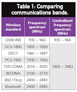
As Table 1 shows, the frequency range of personal wireless communications standards is extensive. As a result, a double-resonant input matching network for the LNA/mixer was designed to resonate at center frequencies within 935 to 960 MHz and 1805 to 2483 MHz, respectively. The input architecture helps to achieve good impedance matching within these bands and to suppress noise induced in the frequency band between these two spans, without need of an additional notch filter. The front-end circuit incorporates both current-reuse and forward-body-bias techniques in order to minimize current consumption at low supply voltages. In particular, the circuit reuses bleed current from the mixer to energize the LNA15 and a local-oscillator (LO) signal forward-body-bias technique to minimize current draw, while maintaining good electrical performance.
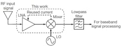
Figure 1 shows the block diagram of an ultra-low-power RF receiver. RF input signals enter the LNA from the antenna. The LNA amplifies these voltage input signals by reusing bleed current from the mixer. Amplified signals from the LNA enter the single-balanced mixer and are mixed with the LO signals. The intermediate-frequency (IF) output signals from the mixer are processed by the lowpass filter. Finally, the filtered signals enter the baseband signal system for further processing.
1. This block diagram shows how the low-power receiver might be used in a communications system.
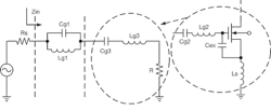
Figure 2 shows the proposed multiple-standard low-power CMOS RF receiver front-end circuit. It contains a stacked NMOS LNA and a single-balanced PMOS mixer. To minimize power consumption, the front-end employs current-reuse and forward-body-bias techniques, although these techniques will not degrade noise figure or linearity. Traditional multiple-standard receivers usually gained good input impedance matching by means of a wideband matching network5 or tunable frequency matching network.16 The former will induce some extra interference in some useless frequencies, which are covered by the wideband matching network;the latter increases the operating complexity of the circuits. The front-end circuit adopts a double resonance matching network to realize the multiple-standard input impedance matching.
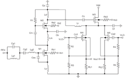
2. This is a more-detailed block diagram of the low-power receiver front end showing its circuit elements.
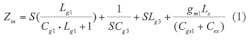
As shown in Fig. 2, the parallel Lg1 - Cg1 and series Lg2 - Cg2 resonances are series connected. For design flexibility, a source degeneration inductor, LS, is placed in series with the source. a capacitor, Cex, is added in parallel with the gate-source of the amplifying transitor, M1.
3. This is an equivalent-circuit diagram of the receiver’s input circuitry and its double-resonator matching network.
In Fig. 3, the source degenerate topology is replaced by its equivalent circuit. The input impedance can be expressed as:
where:
gm1 = the transconductance of transistor M1 and
Cgs1 = the gate-source capacitance of transistor M1.
The values of capacitor Cg3 and inductor Lg3 can be calculated by Eqs. 2 and 3:
Parameter Zin synthesizes an input impedance with a real part equal to gm1LS/Cn, where capacitance Cn = Cex + Cgs, to be matched with source resistance, RS = 50 Ω.
To achieve the required input impedance matching at the desired frequency bands, resonances Lg1 - Cg1 and Lg3 - Cg3 are designed to resonate at center frequencies within 935 to 960 MHz and 1805 to 2483 MHz, respectively. In this way, the input circuit not only accomplishes better impedance matching in both bands of 935 to 960 MHz and 1805 to 2483 MHz, but also suppresses interference within the middle band from 960 to 1805 MHz without using an additional notch filter. The values of the resonating inductors and capacitors can easily be calculated by using the equation ω = 1/2π(LC)0.5.
This file type includes high resolution graphics and schematics.
To achieve a low-power design, the current-reuse technique was used twice in the front-end circuit. In one instance, it was applied to the two-stage cascade common-source LNA. As was shown in Fig. 2, the signal amplified by device M1 is coupled to the gate of device M2 by capacitor Cm while the source of M2 is bypassed by capacitor Cb. The inductive load Lm and LD of the first and second amplifier stages can help to achieve high power gain; the supply voltage will not be influenced, as the voltage drop across them is negligible. Resistor R1 is added to supply a DC bias for device M2. By applying M1 and M2 to share the same bias current, the power consumption of the LNA is minimized. Body effects and parasitic capacitances are not considered. The voltage-transfer function of the first and second stages can be expressed by Eqs. 4 and 5:
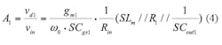
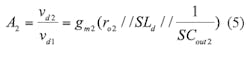
where:
Coutn = the output capacitors (where n = 1, 2) for M1 and M1;
ron = the output resistance for M1 and M2; and
ω0 = the working frequency.
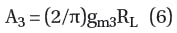
The supply current of the LNA is obtained from the bleed current of the mixer, rather than from the DC source. By doubling the instance of the current-reuse approach, current consumption is minimized while bleeding the current from the mixer helps to improve the conversion gain of the mixer. Device M3 is the transconductance transistor, r while Cp and Cc are the bypass and coupling capacitors, respectively. Inductor Lr and parasitic capacitance Cf at the common source node of the mixer’s switching transistors, M4 and M5, are chosen for values to improve the interstage impedance matching between the LNA and the mixer. The Lr - Cf resonance also helps to suppress 1/f noise at the mixer’s output port. Resistors RL1 and RL2 are load resistors. The conversion voltage gain of the mixer can be found from Eq. 6:
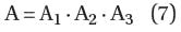
Therefore, the overall voltage conversion gain of the RF front end can be calculated from Eq. 7:
To achieve further savings in power consumption and ensure the feasibility of current reuse between the LNA and the mixer, the supply voltage of the LNA and mixer should be decreased. Usually, the conventional method for accomplishing this is by making the transistors work in their weak inversion regions, although this can degenerate noise figure and gain performance levels. Thus, the forward-body-bias technique is applied to solve this weak point. Typically, the threshold voltage (Vth) equations for both NMOS and PMOS transistors are given as 13:
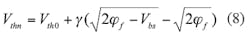
where:
Vth0 = the threshold voltage when Vbs = 0;
γ = the body-effect coefficient;
φf = the bulk Fermi potential; and
Vbs = the voltage between the body and source.
From Eqs. 8 and 9, Vth can be modified by changing Vbs. Thus, the MOS transistors can achieve a dynamic threshold voltage. Since a forward body bias effectively lowers the threshold voltage, the MOS transistors can operate at a reduced bias voltage while maintaining equivalent device characteristics in terms of gain, noise figure, and linearity. However, as the forward body bias turns on the source-to-body junction of the MOS transistors, a DC current flows across the junction with an exponential dependence on the body voltage, leading to additional power consumption and possible latch-up failure. To prevent excessive junction conduction, a current-limiting resistor should be included at the bodyterminal.
By adding suitable positive voltages (Vb1 and Vb2) and current-limiting resistors (Rb1, Rb2) to the body terminals of devices M1 and M2, a forward-body-bias architecture is formed in the front end. From Eq. 8, with the increase of Vbs and the decrease of Vthn, the NMOS transistors can work in a strong inversion region under low-bias-voltage conditions. The stacked NMOS LNA can operate at reduced supply voltages as low as 0.6 V, which is convenient to reuse the bleeding current when the supply voltage is equal to the drain voltage of transconductance transistor M3.
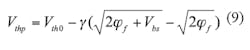
Additionally, a positive voltage (Vb3) and a current-limiting resistor (Rb3) is added to the body terminal of PMOS transistor M3. As Eq. 9 shows, Vbs is then increased and Vthp is decreased, so that the PMOS transistors also work in a strong inversion region under low-supply-voltage conditions.
The mixer employs a novel forward-body-bias method for the switching transistors. The mixer is heavily dependent on the ideal characteristics of the switching transistors, so a local-oscillator (LO) signal forward-body-bias technique is adopted to improve the switching characteristics of devices M4 and M5. The LO voltage is connected to the body terminals of transistors M4 and M5, which can maintain the same waveform and phase, and reduce the voltage amplitude by divider resistors R2/R3 and R4/R5. The body voltage is then cyclical changed with the LO signal, which can be determined by means of Eq. 10:
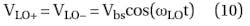
From Eq. 9, when VLO+ > 0 and VLO- < 0, the value of VG for device M4 increases, and | VGS| declines and |Vthp| increases, which accelerates the PMOS transistor to satisfy the cutoff condition that |VGS| < |Vthp|, and device M4 enters the cutoff state quickly.
At the same time, the value of VG for device M5 declines, |VGS| increases and |Vthp| declines, accelerating the PMOS transistor to satisfy the turn-on condition, |VGS| > |Vthp|, and device M5 enters the turn-on state quickly. The LO signal is coupled to the body terminal and enables the threshold voltage to change in a cyclical manner. This not only helps the mixer to work at low power consumption, but also raises the switching speeds of the transistors. The switching characteristics of the active devices is nearly ideal, and the noise figure and linearity are improved considerably.
The thermal noise is greatly generated when switching transistors turn-on simultaneously. The average noise current within one LO period can be expressed by means of Eq. 11:
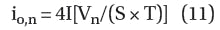
where:
Vn = the 1/f noise of the MOS transistor;
T = the cycle time of the LO;
I = the DC current of the switching transistor; and
S = the LO signal slope at point zero.
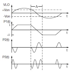
4. These plots show the resulting waveforms for P1(t), P2(t), and P3(t) for an applied LO voltage.
Parameter S is critical to noise performance: a larger value of S means smaller noise current. Parameter S can be increased to improve the switching characteristic, so it is propitious to reduce noise current.
Linearity is an important performance of RF front-end, especially for the last stage of the whole circuit. Thus, the linearity of this front-end circuit is greatly influenced by the switching transistors M4 and M5. Their output current, i0, has a nonlinear relationship with input voltage vs, which can use the Taylor series to expand as shown in Eq. 12:

From Eq. 12, where pn is the derivative of i0 ~ Vs, the typical waveform is shown in Fig. 4. When the switching transistor is on, p1(t) = 1, p2(t) = p3(t) = 0, while in the switching time period Δ, p1(t), p2t), p3(t) are unequal to zero. The voltage mode for the input third-order intercept point, VIIP3, can be analyzed by means of Eq. 13:
From Eq. 13, it can be concluded that smaller values of |p3| mean higher IIP3 and better linearity. With the aid of the LO signal forward-body-bias technique, the switching time, Δt, is reduced, implying that the time for |p3| ≠ 0 is reduced and the IIP3 performance of the circuit has been enhanced considerably.
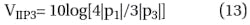
5. The front-end receiver’s S11 response was simulated from 0.6 to 2.6 GHz.
The RF receiver front-end design was implemented in the 0.18-μm silicon CMOS process at the foundry of the Taiwan Semiconductor Manufacturing Company (TSMC). By using the forward-body-bias technique, the receiver’s supply voltage drops to 1 V when the forward body bias voltages are chosen at Vb1 = Vb3 = 0.4 V and Vb2 = 0.35 V. Operating across the frequency ranges of 935 to 960 MHz and 1805 to 2483 MHz, the input reflection coefficients S11 for those frequency ranges are less than -14 and -11 dB, respectively, as shown in Fig. 5.
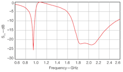
6. The front-end receiver’s double-sideband (DSB) noise figure was simulated from 0.6 to 2.6 GHz.
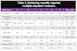
The double-sideband (DSB) noise figures range from 2.3 to 2.4 dB and 2.7 to 5.1 dB, respectively, across those two frequency bands, as shown in Fig. 6. The conversion gains for the two frequency ranges are 18.6 to 19.0 dB and 18.7 to 20.8, respectively (Fig. 7). The input third-order-intercept points (IIP3) for the front end are -8.2 dBm at 935 MHz and -9.8 dBm at 2100 MHz (Fig. 8). Figure 9 shows the layout for the front end, with an active area of 0.61 x 0.53 mm2. The power consumption is only 2.1 mW—considerably lower than with comparable-frequency RFICs. Table 2 summarizes the performance of the front-end device compared to recently reported devices for similar wireless multiple-standard application.
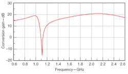
7. The conversion gain of the front-end receiver was simulated from 0.6 to 2.6 GHz.
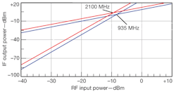
8. The input third-order-intercept (IIP3) response of the front-end receiver was simulated at 935 and 2100 MHz.
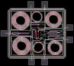
9. This chip photograph shows the basic layout of the dual-band front-end receiver, which was fabricated in a commercial silicon CMOS foundry.
By adopting current-reuse and forward body bias techniques, the total measured conversion gain of the receiver is 18.6 to 20.8 dB and the double-sideband noise figure ranges from 2.3 to 5.1 dB across the frequency range. The IIP3 is -8.2 dBm at 935 MHz and -9.8 dBm at 2100 MHz. The power consumption is a mere 2.1 mW while operating with a 1-V supply.
Kui Fu, Masters Degree Candidate
Xiarong Guo, Professor
Chunhua Wang, Professor and Doctoral Supervisor
Yuxiang Tu, Doctorate Degree Candidate
Chishi Liu, Masters Degree Candidate
College of Information Science and Engineering, Hunan University, Changsha 410082, People’s Republic of China; e-mail: [email protected].
Joe McGeehan, Professor
Center for Communication Research, University of Bristol, Bristol, BS8 1UB, United Kingdom; www.bris.ac.uk.
Acknowledgment
The authors wish to thank the Open Fund Project of the Key Laboratory of Hunan University (No. 12K012).
References
1. J. Liu, H. Liao, and R. Huang, “0.5 V ultra-low power wideband LNA with forward body bias technique,” Electronics Letters, Vol. 45, No. 6, 2009, pp. 289-290.
2. T.T.N. Tran, et al., “Ultra-low-power series input resonancedifferential common gate LNA,” Electronics Letters, Vol. 47, No. 12, 2011, pp. 703-704.
3. W. Dake, et al., “A 0.4-V Low Noise Amplifier Using Forward Body Bias Technology for 5 GHz Application,” IEEE Microwave and Wireless Components Letters, Vol. 17, No. 7, 2007, pp. 543-545.
4. A. Chyuen-Wei, Z. Yuanjin, and H. Chun-Huat, “A Multi-bandCMOS Low Noise Amplifier for Multi-standard Wireless Receivers,” in ISCAS 2007 IEEE International Symposium on Circuits and Systems.
5. W. Hongrui, Z. Li, and Y. Zhiping, “A Wideband Inductorless LNA With Local Feedback and Noise Cancelling for Low-Power Low-Voltage Applications,” IEEE Transactions on Circuits and Systems I: Regular Papers, Vol. 57, No. 8, 2010, pp. 1993-2005.
6. W. Chao-Shiun, L. Wei-Chang, and W. Chorng-Kuang, “A multi-band multi-standard RF front-end IEEE 802.16a for IEEE 802.16a and IEEE 802.11 a/b/g applications,” in IEEE 2005 International Symposium on ISCAS.
7. N. Mingchen, et al. “A wide-band RF front-end for multi-standard application,” in 9th International Conference on Solid-State and Integrated-Circuit Technology, ICSICT 2008.
8. L. Chen-Ming, et al., “A Low-Power Self-Forward-Body-Bias CMOS LNA for 3-6.5-GHz UWB Receivers,” IEEE Microwave and Wireless Components Letters, Vol. 20, No. 2, 2010, pp. 100-102.
9. G. Sapone and G. Palmisano, “A 3-10-GHz Low-Power CMOS Low-Noise Amplifier for Ultra-Wideband Communication,” IEEE Transactions on Microwave Theory and Techniques, Vol. 59, No. 3, 2011, pp. 678-686.
10. D.K. Shaeffer and T.H. Lee, “A 1.5-V, 1.5-GHz CMOS low noise amplifier,” IEEE Journal on Solid-State Circuits, Vol. 32, No. 5, 1997, pp. 745-759.
11. H. Chih-Lung and H. Yi-Lun, “A low supply voltage dualband low noise amplifier design. in Consumer Electronics,” IEEE 13th International Symposium on ISCE, 2009.
12. C. Chieh-Pin, et al., “A High Gain and Low Supply Voltage LNA for the Direct Conversion Application With 4-KV HBM ESD Protection in 90-nm RF CMOS,” IEEE Microwave and Wireless Components Letters, Vol. 16, No. 11, 2006, pp. 612-614.
13. C. Chieh-Pin, C. Ja-Hao, and W. Yeong-Her, “A Fully Integrated 5 GHz Low-Voltage LNA Using Forward Body Bias Technology,” IEEE Microwave and Wireless Components Letters, Vol. 19, No. 3, 2009, pp. 176-178.
14. J.F. Chang and Y.S. Lin, “0.99 mW 3-10 GHz common-gate CMOS UWB LNA using T-match input network and self-body-bias technique,” Electronics Letters, Vol. 47, No. 11, 2011, pp. 658-659.
15. L. Viet Hoang et al., “Current-Reused Ultra Low Power, Low Noise LNA+Mixer,” IEEE Microwave and Wireless Components Letters, Vol. 19, No. 11, 2009, pp. 755-757.
16. E.C. Becerra-Alvarez, J.M. de la Rosa, and F. Sandoval, “Design of a 1-V 90-nm CMOS folded cascode LNA for multi-standard applications,” in 53rd IEEE International Midwest Symposium on Circuits and Systems (MWSCAS), 2010.
This file type includes high resolution graphics and schematics.
