VNAs Must Keep Pace with Advanced Signal-Integrity Demands

This article is part of the TechXchange: Vector Network Analyzers.
What you’ll learn:
- The need for signal integrity in high-speed digital designs.
- How VNA testing can help achieve performance demands.
Maintaining signal integrity (SI) in high-speed digital designs is becoming a more daunting task with the rollout of each new technology generation. As data rates reach 128 Gb/s and beyond, printed-circuit-board (PCBs) space diminishing, and system designs shrinking in size, engineers need advanced test solutions that support high frequencies.
Vector network analyzers (VNAs) have become the instrument of choice for many SI engineers. However, the analyzers must provide proper frequency coverage and have specific SI analysis tools to conduct accurate, repeatable measurements.
What Causes Signal Degradation?
Engineers conduct signal-integrity measurements to ensure the quality of an electrical signal meets designated industry standards. Signal integrity specifically addresses issues related to channels on parts such as backplanes, PCBs, connectors, cables, as well as active components in the serializer and deserializer (SerDes).
Signal quality is degraded by quantities such as the loss of amplitude, crosstalk, delay, jitter, noise, and interference. Signal degradation on a PCB can be caused by a number of factors, most notably those listed in the table.

Benefits of VNAs in Signal-Integrity Verification
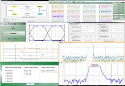
VNAs hold significant advantages over traditional time-domain-reflectometry (TDR) measurement equipment, especially as speeds ramp up. Proper SI VNAs incorporate the capabilities of TDR and impedance equipment, but they also provide improved electrostatic-discharge (ESD) protection as well as support frequency- and time-domain testing, including TDR, impedance, and Delta-L (Fig. 1). VNAs also allow for automatic measurements to be made to save time and improve repeatability.
Moreover, VNAs have more extensive functionality with better specifications to support differential testing for high-speed backplane applications. On top of that, certain VNAs for SI applications maintain a more flexible compact hardware architecture that includes two receivers per port in a more robust single-chassis construction.
Choosing the Correct VNA Frequency
When selecting a VNA for signal-integrity designs, frequency coverage is an important consideration. There’s a correlation between the analyzer’s frequency range and the clock rate of the signal.
For example, a 40-Gb/s system uses a 20-GHz NRZ (non-return-to-zero) clock. During development, a design engineer needs to measure the 3rd or 5th harmonic of the NRZ to characterize performance. A VNA that covers up to 40 GHz can be used to conduct measurements on the system. Measuring the 3rd harmonic of a 25-Gb/s system can be performed with a 40-GHz analyzer.
To support emerging high-speed designs, PAM4 modulation replaces NRZ. One advantage of PAM4 is that it doubles the bit rate for a given baud rate compared to NRZ. The tradeoff is the signal-to-noise (SNR) ratio is higher, making the signal much more sensitive to noise.
To support 112-Gb/s PAM4, the VNA frequency must extend to 43.5 GHz, and for a 224-Gb/s PAM4 signal, a VNA with frequency coverage up to 70 GHz is necessary. Equally important is the lower-end frequency of the VNA, as it can significantly improve modeling. For example, a 70-kHz start frequency reduces the risk of DC extrapolation errors for more accurate models. The result is fewer design turns, improving time and cost efficiencies.
VNA Tools for Signal Integrity
VNAs also need to provide specific test capabilities for SI designs. At a minimum, the VNA must support TDR-like measurements, so that the analyzer can accurately identify impedance discontinuities and other faults in data transmission cables, backplanes, and other devices under test (DUTs).
Dedicated software for network extraction and embedding/de-embedding are also valuable analysis tools for SI designs. Network extraction identifies and removes subsets of a structure, such as a test fixture, PCB, and other interconnects that behave as localized pseudo-lumped-element reflection centers.
Sequential peeling is a model/measurement-based method of network extraction for de-embedding that helps analyze isolated defects within a test fixture or other complex network. The sequential-peeling technique acquires detailed information about the fixture, making it easy to improve the test fixture design and, ultimately, first-time yields.
Sequential peeling is particularly useful for electrically small structures with isolated vias in the transmission-line runs, such as on PCBs. That’s because sequential peeling identifies time domain elements and then fits a shunt admittance or series impedance model to the isolated data. Once a series of these elements are identified, a more complete composite model of the structure can be obtained and de-embedded.
Delta-L Solves PCB Test Issue
Developing dedicated software that supports Delta-L enables VNAs to efficiently verify high-speed designs. Delta-L is an algorithm developed by Intel, whereby PCB manufacturers can validate their products. The VNA serves as an important requirement for all PCB makers to comply with Delta-L testing and satisfy the link budget for backplane design on Intel servers.
The key benefit of Delta-L is that it removes the effects of probes and via holes by measuring two different lengths, simplifying and improving the accuracy of acquiring PCB characteristics. When the Delta-L software is installed, the VNA can measure insertion loss within differential pairs, and uncertainty of insertion loss, impedance, and effective dielectric constant for PCBs (Fig. 2).
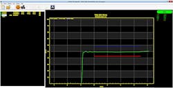
Insertion loss is a key measurement, especially in emerging high-frequency designs. The higher the frequency, the greater the losses. When the insertion loss falls below the specified threshold, the signal is lost.
Conclusion
As high-speed designs incorporate next-generation technologies, VNAs will continue to serve as a key tool during verification. For engineers to have confidence in their high-speed designs, selecting an analyzer that has the proper frequency coverage and dedicated SI measurement tools are necessary for accurate and repeatable results that will save time and money.
Read more articles in the TechXchange: Vector Network Analyzers.
About the Author
Navneet Kataria
Product Marketing Engineer, Anritsu Co.
Navneet Kataria is a Product Marketing Engineer at Anritsu Company. He has 10 years of experience in test and measurement, serving various technical and business roles.
