11 Myths About the PCB Industry

What you’ll learn:
- PCB design is not a simple exercise in which one size fits all.
- High-data-rate, high-frequency designs provide very little “wiggle” room in terms of performance constraints.
- If you have a failed design, you must start the process all over again.
Printed circuit boards (PCBs) have been around so long that product developers often think their design, manufacturability, and reliability is a “no-brainer.” It’s widely assumed that the value in any modern electronic product is driven by the components mounted on the board and the software applications embedded within these components.
However, today’s high-frequency, high-data-rate devices are challenging these long-held assumptions such that a successful PCB implementation has once again become one of the focal points in the overall product development process. Below are some long-held myths associated with board development.
1. PCBs are commodities and essentially just the “carriers” for the ICs mounted onto them.
Yes, it’s true. For a long time, PCBs were not a huge area of concern. There was lots of “wiggle room” in the roles that various aspects of board technology and materials played in the overall end-product design, so getting the PCB design “kind of right” often sufficed. But, as we began moving up the speed curve (starting at about 2.5 Gb/s), any margin for error in board design disappeared. As we climb further up the curve, such latitude for creating a board that works right the first time and every time thereafter shrinks.
Now with today’s high-frequency, high-data-rate designs, the tolerance for any kind of misstep has essentially evaporated. More importantly, there are no “do-overs” with today’s fine-pitch components. If your board fails, it’s not just the board you lose. You’re also losing components that can cost tens of thousands of dollars. On top of that, there’s the loss of revenue resulting from being late to market, or not having a sufficient service life to provide long-term revenue and profitability.
2. The PCB design process is very straightforward.
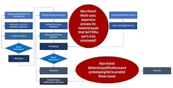
Of course, certain electronic devices don’t require a complex board design (anything more than eight layers). But for today’s high-frequency, high-data-rate products, PCBs are the critical foundation upon which all other design development requirements are built. Figure 1 depicts the flow of a typical design and fabrication process. As shown, PCB design and fabrication involve a multistep process wherein errors can occur in any stage.
Think of it in terms of building a house. The foundation may initially look fine, but if it’s not successfully designed and built from the outset, building atop it could result in a catastrophic failure of the whole structure.
3. PCBs don’t contribute to the overall operation of the end products into which they’re incorporated.
In complex designs, the PCB’s design and the characteristics of the constituent laminate material play a huge role in the end product’s performance. The three main laminate characteristics that factor into design, manufacturability, reliability, and lifespan of a product are impedances, losses, and skew.
However, each of those characteristics has subsets, and in the final analysis at least 10 different material characteristics come into play when you’re developing a high-frequency, high data-rate design. Ignore them at your own peril—any one of them might be enough to throw your entire product design off the rails.
4. EDA tools make PCB design a “pushbutton” process.
In the late 1980s and early 1990s, the plethora of EDA toolset providers would have their customers believe that a particular toolset (or suite of toolsets) could automate the PCB design process. For example, EDA vendors often crowed that their toolsets could autoroute 90% of a given PCB design. Maybe so, but left unsaid was that the last 10% of the routing was often the most difficult and time-consuming aspect of the job.
The other part of the EDA vendors’ marketing mantra was that a suite of toolsets from one vendor would address all of your PCB design needs. But savvy engineers knew it was unwise to leave your PCB design to a suite of EDA toolsets.
Rather, they understood that successful design of manufacturable and reliable PCBs was best achieved using optimized point tools. Even today, the engineers who are most successful with their high-frequency, high-data-rate designs pick and choose those point tools they know will most likely realize their targeted, fully functioning, completed design.
Also, PCB tools have often been the “red-headed stepchildren” within a suite or family of EDA tools. The focus has long been, and continues to be, on components, their characteristics, and how best to leverage them within a design. The PCB tools within a given vendor’s toolsets often come by way of corporate acquisitions. And, while their performance may have sufficed at the time of that acquisition, they may not keep up with emerging design challenges in the longer run.
5. It’s difficult to have visibility into the fabrication process when designing a PCB.
While this statement was true in the past, there are EDA tool providers who more closely link the PCB design and manufacturing processes together. Several factors and datasets come into play during the manufacturing process that can influence the board-design process. Included among them are resin content, dimensional stability, and glass weave.
The biggest challenge is educating designers on those aspects of the fabrication process that can affect their designs. To this end, we need more synergy between the design and fabrication processes, and more sharing of information on those aspects of PCB manufacturing that can create hidden “gotchas” in the end products.
6. Multiple re-spins of PCBs are an accepted way of doing product development.
In truth, this statement is less a myth and more the “traditional” way of doing business in the PCB industry. In decades past, the only way to verify your PCB design was to fabricate a prototype for population and testing. If issues arose, that meant going back to the drawing board. This process was repeated time and again until there was a working PCB.
Even worse, sometimes a seemingly correctly designed board was manufactured in volume only to have some or even all of them fail in the final product. The result of such calamities was high NRE costs, lost time to market, and lost competitive advantages that caused profits to suffer.
Thus, the industry came to accept multiple re-spins of a board as standard operating procedure. Sadly, many OEMs still accept multiple PCB re-spins as part of the cost of doing business. This way of thinking can infect the product-development process from the start with the notion that a completely optimized board design is unachievable. As a result, the PCB development process often avoids much-needed attention or scrutiny.
7. Designing the PCBs used in today’s high-frequency, high-data-rate designs has lots of “wiggle room.”
The fact is that today’s high-frequency, high-data-rate products have left very little wiggle room in the PCB design process, particularly in the arena of board stackup. In 112-Gb/s/channel and 5G/mmWave applications, a slight misstep can quickly render a design inoperable or unmanufacturable.
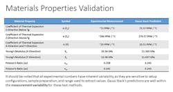
A complete stackup design is one that includes fully integrated electromagnetic and thermomechanical simulations. A technically correct and financially optimized design approach is one that affords accurate prediction of resin starvation and glass-stop issues, and it provides board-level thermomechanical properties including coefficients of thermal expansion in all directions—X, Y, and Z axis (both above and below Tg). With that information in hand, the designer can more accurately predict the board’s reliability and performance.
8. Beyond dieletric constant (Dk) and low loss (DF), there’s not much insight as to how other material characteristics will affect a PCB.
While this was true in the past, more insight is available today, especially with the growth of high-frequency, high-data-rate designs. While more information is always good, the ability to put meaning behind the information becomes the crucial factor within the process.
9. The material information provided from laminate vendors is complete.
Dk and DF information has long been available from laminate vendors and, by and large, that information is reliable and reasonably complete. The challenge involves extending information beyond those two properties.
Mechanical properties as a function of construction haven’t been available. In effect, each stackup presents different properties, even when built on the same material, and this can have serious implications for the manufacturability and reliability of the board. Often, material test vehicles are used to qualify a particular material, but each stackup may behave very differently from the test vehicle.
The characteristics shown in Figure 2 go far beyond the typical Dk and DF information typically provided by material suppliers. They all can impact the final design, manufacturability, and long-term reliability of the PCB.
10. It doesn’t require lots of training to become proficient in using EDA tools that address complex design elements such as signal integrity.
More than a few EDA tools utilized for critical issues like signal integrity have been difficult to use and require a lot of expertise to obtain the relevant data. Because these toolsets aren’t employed on a day-to-day basis, it’s not unusual for engineers to have to “relearn” the tool each time they undertake a new PCB design.
Getting up to speed can exceed the product-development timeline. It may also enable errors to creep into the process because the engineer using the tool is not fully familiar with its operation and doesn’t know when to question critical results.
11. New or updated EDA tools all have the same construct and are based on the same internal technology.
In many instances, revisions to existing toolsets or the creation of new ones has focused on adding more information, often in the form of libraries. While more information is always better, all libraries aren’t created equal. Often, it’s difficult to ascertain which data is good or bad.
Without the ability to manipulate data in a meaningful way or to use a new construct (like a new algorithm or simulation capability) to better leverage the vast set of information within a toolset, the benefits realized from a “revised” or “brand-new” toolset may fall far short of what’s required by today’s product developers. This is especially the case for high-frequency, high-data-rate products.
In addition, the ability to provide EDA design services via an online, pay-as-you-go business model can result a highly effective and reliable PCB design environment. Such approaches meet the needs of many PCB product developers who don’t require a resident toolset and lack the budget to pay for a yearly subscription “per-seat” license that’s the norm with many EDA toolset providers.
About the Author
Kella Knack
Director of Strategic Marketing, Avishtech
Kella Knack currently serves as Director of Strategic Marketing for Avishtech, a leading provider of EDA software design tools—Gauss Stack and Gauss 2D. She assists in the company’s marketing communications, PR, and outbound messaging efforts.
Previously, she served as Vice President of Marketing for Speeding Edge, an engineering consulting and training company focusing on the design of high-speed PCB and system design. Before that, she was the Founder and President of KJ Communications, Inc., a marketing consulting and public-relations company based in Silicon Valley. She served as a strategic adviser for several highly successful marketing campaigns for clients that ranged from startups to multimillion dollar companies in the EDA, networking, SOC IP, semiconductor, embedded-system design, and database-management market sectors.
