Extending RF’s Boundaries via Direct Data Sampling in the Ka-band

Download this article in PDF format.
What you’ll learn:
- How and why fmax hit a wall at the 28-nm node.
- Progress in RF signal-chain innovation will come not on ASICs but on FPGAs.
- Developments in direct data-conversion devices will pave the way to SDM air interfaces.
It’s widely recognized that software-defined microwave (SDM) air interfaces have huge potential. Through this technology, it will be possible to revolutionize many different aspects of the communications arena by making major transformations to the infrastructure that it relies on. More specifically, it’s certain to be of great benefit in the space sector. That’s because it will be possible to finally alleviate the highly frustrating cycle-time mismatch in the rates of progress in ground- and space-based hardware development.
Rather than having to utilize hardwired, overly hardware-centric solutions, which can quickly become outdated, it will be feasible for space-borne assets to be reconfigured while in orbit. As a result, they will be able to deal with different workloads or provide different services, depending on where they are at any given time.
For instance, when their low-Earth-orbit (LEO) travel path takes them over densely populated regions, they could provide broadband connectivity in various frequency bands depending on the atmospheric conditions or the available frequencies. Conversely, as they overfly a desert or an ocean, their highly software-centric RF system and processing resources could be switched to focus on another task (e.g., providing a radar-based earth observation service and analyzing captured imaging data, and so on) using the same hardware and the same overall system operator investment.
Such multi-mission capability would mean that service provision could be better balanced with demand. In addition, the cost barriers that prevent deployment of satellites for certain activities might be substantially reduced (as these activities could be piggybacked with other services).
The purpose of this article is to describe exciting new developments underway within the RF signal-conditioning domain that are bringing us closer to an SDM era. We will look at the growing impetus to push direct data sampling deep into the Ka-band.
RF Semiconductor Technology Today
It must be acknowledged that RF innovation in its conventional form is reaching some hard limitations. For more than two decades, the price points associated with software-defined baseband radio technology have benefited from the ongoing cost reductions of volume CMOS manufacturing processes, in line with the principles of Moore’s Law. Iterative technological progression has translated in improved performance, reduced power consumption, and support for a widening breadth of functionality.
As the advances that can be made through downsizing alone become more difficult, with physical constraints at a nanoscale level having an acute impact on the validity of Moore’s Law, new approaches will need to be found.
The latest semiconductor nodes are too small to support construction of the high-performance RF front-end sampling systems needed in the market. Furthermore, the costs involved in developing next-generation semiconductor processes with finer architectures will only be economically viable for ultra-high-volume sectors (such as consumer electronics and data-center infrastructure). It will not be applicable to numerous medium-volume industrial applications and other more specialized areas.
A key figure of merit (FOM) for any RF device is its maximum frequency (fmax), which is the frequency at which transistor power gain falls back to one. For years, the achievable fmax had risen, reaching higher frequencies with shrinking transistor gate sizes. The peak for fmax came at the 28-nm process node (with figures of around 360 GHz being witnessed). Since then, further improvements in fmax have been hard to come by. At the 14-nm process node, fmax values more than halved compared to what was possible at 28 nm (approximately 160 GHz).
Numerous factors have contributed to the decline in fmax at smaller process nodes. Among these are the increasing potency of parasitics. Furthermore, there’s the effect that reduced threshold voltages has on parameters like dynamic range and noise levels. Against this backdrop of rapidly diminishing analog returns, concerns have arisen: How will the semiconductor industry continue to support future RF ingenuity?
Much of the research work conducted during the last decade has focused on enhancing BiCMOS capabilities, as well as the development of heterojunction bipolar transistors (HBTs) based on silicon-germanium (SiGe) semiconductor substrates. Such work has demonstrated that SiGe HBTs offer significantly higher cutoff frequencies, higher output power, and superior analog characteristics versus those of CMOS field-effect transistors (FETs) that are fabricated on the same process node. The integration of SiGe HBTs into CMOS platforms therefore presents an attractive approach, promising boosts in RF performance.
A Shift to Programmable Logic
Due to the prohibitive costs, it’s become impossible for further RF signal-chain innovation to occur using only custom ASICs as its foundation. Rather, the industry must turn to mixed-signal front ends implemented using today’s state-of-the-art FPGAs—there’s much room for development of superior signal-processing capabilities using this approach. It’s in this context that the RF sector is seeing growing interest in advanced system-in-package (SiP) solutions. Incorporating SiPs might give rise to significant miniaturization of mmWave RF systems.
Mitigating the parasitics in microwave devices will require use of state-of-the-art packaging materials. In the past, low-temperature co-fired ceramic (LTCC) substrates would typically be employed, but as we migrate toward the Ka-band (26 GHz and above), we must turn to organic substrates.
An Overview of SDM Developments
After identifying trends that would influence RF technology going forward, Teledyne e2v’s engineering team began work on direct-sampling technology for microwave implementations. In addition to the SDM possibilities it offers, direct sampling provides additional benefits such as eliminating the need for frequency conversion, which would in turn curb signal distortion.
Initial experiments in the summer of 2019 centered on a K-band-capable quantizer prototype. For those early trials, the setup combined the company’s existing EV12AQ600 quad-core analog-to-digital converter (ADC) with its RTH120 ultra-high-frequency track-and-hold amplifier (THA). The ADC offered 6.4-GS/s operation, while the THA provided strong linearity plus bandwidth out to 24 GHz.
Throughout 2020, progress led to a series of prototypes. By time-interleaving a pair of EV12AQ600 ADCs, the sampling rate doubled to 12 GS/s, yielding the results shown in Figure 1. Sampling a 25-GHz input signal at 10-GS/s rate results in second- and third-harmonic spurs at −56 dB and −57 dB, respectively. We found that moving to single-ended signal and clock lines greatly facilitates integration of the hardware into customer systems, an approach taken in subsequent prototypes.

Encouraged by the K-band data, the next phase comprised experiments at Ka-band frequencies. Rather than basing such work on existing ADC components, Teledyne e2v engineers created a new proof-of-concept device, the EV12PS640. This 12-bit ADC SiP supports 12-GS/s operation and features an organic, low-dielectric substrate. Its compact form factor (33 × 19 mm) consumes minimal board space.
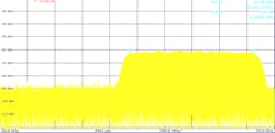
To complement its advances in ADC technology, the company is also looking to improve digital-to-analog converters (DACs). Like the EV12PS640, its 12-bit EV12DD700 dual-channel device has high-frequency direct-sampling capabilities and supports 12-GS/s operation at 30 GHz. Other supported functions include direct digital synthesis (DDS) and digital upconversion (DUC) via a pair of built-in, 32-bit, numerically controlled oscillators (NCOs). The spurious-free dynamic range (SFDR) plot in Figure 2 illustrates its performance from 20 to 25 GHz.
In common with earlier DAC solutions, the EV12DD700 features multiple output-coding modes. This makes it possible to tailor output power characteristics to the precise position within the spectrum where synthetic signal bandwidth is required (Fig. 3).

Beyond its single and multi-tone generation capabilities, the EV12DD700 DAC is well-positioned to provide support for highly agile and responsive frequency hopping (including multi-mode hopping). Return-to-zero (RTZ), continuous, and coherent modes are all built into this device.
Frequency-hopping control can either be managed through the standard serial peripheral interface (SPI) or via dedicated serial-data lines that deliver accelerated reaction times. Through use of the DDS mode, the two on-board 32-bit NCOs can locally generate signals, eliminating the need for continuous data flow from a signal processor. This pair of NCOs also can be programmed to locally generate radar chirps, thereby helping to minimize data-throughput overhead.
Looking Ahead
Teledyne e2V is preparing to enter the third and final stage of its investigation, before production begins of direct data-conversion devices for the ultra-high-frequency band. By the end of 2021, initial samples of its ADCs are scheduled to be available. The expectation is that these ADCs will deliver top-end bandwidth specifications that are close to 40 GHz. Sampling of the EV12DD700 will continue through the first few quarters of 2021, with the latest round of device improvements underway before production launch.
Conclusion
With such forward-looking data-converter products soon to be available for implementation, the goal of SDM air interfaces is now clearly on the horizon. With this in mind, RF engineers should begin planning how they will transition to data-conversion architectures that will accommodate this technology.
Check out these videos of the first demonstration of the Ka-Band ADC proof-of-concept device:
And of the first demonstration of the Ka-Band DAC device:
About the Author
Nicolas Chantier
Marketing Director, Teledyne e2v
Having worked for Teledyne e2v for almost 14 years, Nicolas Chantier heads up the marketing team for its Data & Signal Processing Solutions division. He’s based at the company’s site in Grenoble (France). Prior to joining Teledyne e2v, he worked for National Semiconductor in Germany for 10 years and had previous experience with Kenwood Electronics and Alcatel. Nicolas holds a degree in Engineering from Coventry University (UK).
