Improve Simulation with 3D QFN-Package Models
Members can download this article in PDF format.
What you’ll learn:
- Benefits associated with 3D geometry models.
- How 3D models for QFN packages can help designers.
- Best practices when using 3D package models.
Quad-flat no-leads (QFN) packages are commonly used for RF applications to connect integrated circuits (ICs) to printed-circuit boards (PCBs). The benefits associated with QFN packages include low cost, a small form factor, and good electrical and thermal performance. QFN packages come in various sizes, typically ranging from 3 × 3 mm to 9 × 9 mm.
One company that manufactures QFN packages is Barry Industries, which offers versions rated to 40 GHz. In contrast to plastic QFN packages, Barry builds high-temperature co-fired-ceramic (HTCC) versions that feature low-loss broadband transitions, allowing for superior performance over frequency. These packages also withstand much greater temperatures than plastic QFN packages and can be sealed hermetically.
Barry’s QFN packages come in six sizes that range from 3 × 3 mm to 8 × 8 mm. Each package size is available in any of three different configurations: bare seal ring, grounded seal ring, and castellated grounded seal ring.
Bare seal ring, an epoxy or glass-lid-attachment configuration, is the lowest cost of the three options. Grounded seal ring is a solder-lid-attachment configuration. Castellated grounded seal ring also is a solder-lid-attachment configuration, but it includes castellations that allow solder fillets to form, thus making it possible to visually inspect pin solder joints. This configuration is the most expensive, too.
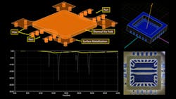
Barry Industries and Modelithics are partnering to offer 3D geometry models for Barry’s QFN packages (Fig. 1). These models are intended for use with Ansys HFSS and are available in the latest version of the Modelithics COMPLETE+3D Library.
In addition to the 3D geometry models, designers should be aware that Modelithics offers equivalent-circuit models for many of these same packages. These equivalent-circuit models were created using Ansys HFSS 3D simulation data after validating EM simulations with lab measurements for several test conditions. In total, 18 Barry QFN packages are represented with both a 3D geometry model and an equivalent-circuit model.
Advantages of 3D Models
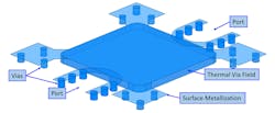
3D geometry models are intended for use in full-wave 3D electromagnetic (EM) simulations. They enable designers to predict coupling effects that can occur when components are located close to other components or objects (3D models for Barry packages predict coupling effects within the package and outside the package body).
However, such effects can’t be captured when using equivalent-circuit models. 3D geometry models, which are included as part of a custom HFSS library, are based on physical dimensions and material properties and are encrypted to protect manufacturer IP.
In the case of the Barry 3D package models, for instance, designers don’t have access to material properties due to encryption but do have access to all package pins—both inside and outside (Fig. 1, again). Therefore, users can load the model in an EM environment and optimize the PCB layout for the best performance (more on this later). Designers can also optimize matching inside the package by utilizing carefully selected wire shapes, ribbons, and so on.
In addition, since designers have access to all pins, the models allow for a great deal of flexibility. Pins can be terminated (inside and outside) as needed to achieve optimal performance. With these 3D package models, designers are able to combine pins for RF signals, utilize certain pins for dc bias lines, and optimize grounding patterns to meet design requirements.
It should be noted that Modelithics 3D package models are well-suited for co-simulations. For example, say a designer has access to a MMIC amplifier’s S-parameter data. The designer could then create a simulation project in which the MMIC amplifier is mounted inside the package. Bond wires would be used to connect the amplifier to the package. Then a co-simulation could be performed that involves simulating the package and bond wires in HFSS. Ports must also be added to enable co-simulation. Subsequently, the MMIC amplifier’s S-parameter data would be connected to the ports to enable a co-simulation.
In a similar manner, 3D package models also can be combined with Modelithics equivalent-circuit models for capacitors. To summarize, the co-simulation process involves combining 3D EM simulation data with S-parameter data or circuit models associated with fast optimization.
Measurement Validations
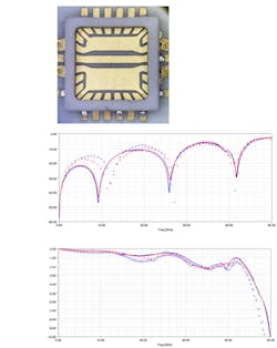
Of course, when possible, it’s recommended to compare simulated results with measured data for additional validation. In this case, we analyzed a 4-mm package with a custom built-in matched line.
Figure 2 shows the package along with graphs that illustrate both simulated results and measured data. We used both microstrip and ground coplanar-waveguide (GCPW) configurations. 3D models can be considered as value-added tools that allow designers to optimize PCB footprints. For this analysis, we optimized performance through proper grounding, which is discussed in detail below.
Performance Hurdles
In broadband package designs, designers may want to have resonance-free performance. The nature of the package geometry results in multiple unwanted resonances. Therefore, several mitigation techniques are recommended to suppress the resonances and achieve best performance. These mitigation techniques have been realized through extensive simulations with the 3D models.
One of the specific features that contributes to the package resonances is pin-to-pin proximity. Specifically, the pins in the QFN-4424-0522 package are located 0.5 mm apart from one another. This 0.5-mm spacing between pins results in strong coupling. Multiple adjacent pins form a periodic structure that results in both higher- and lower-frequency resonances.
Packages that rely on a metallization ring to attach the cover exhibit additional resonances. The next section focuses on removing unwanted resonances within the frequency band of interest.
Techniques for Using the 3D Package Models
As stated, removing the unwanted resonances require several mitigation techniques to be applied. For one, it’s recommended to ground the package pins located adjacent to the RF signal pins both internally and externally. The ground vias should be in the form of a “pin triplet” (to be shown later). Another possible mitigation technique involves attaching a microwave absorber (i.e., Emerson Cummings MF190 or similar) to the metallization in each of the four corners to avoid resonances associated with the metallization ring.
Additional mitigation techniques include grounding the corner pins using the same grounding method applied to the pins adjacent to the signal pins. To ground the corner pins, one should employ enough PCB surface metallization and ground vias. Sufficiently grounding the corner pins helps to suppress the effects of the metallization ring.
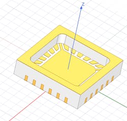
Figure 3 illustrates both how the corner pins should be grounded and the aforementioned “pin triplets” employed to ground the pins adjacent to the signal pins. Grounding of corner pins is available to designers, particularly when pins aren’t used for dc lines or other functions. Therefore, the user can evaluate extended design requirements when using these 3D models.
Analyzing the Package with All Mitigation Techniques
Figure 4 shows a simulation model of the QFN-4424-0522 package implementing all of the mitigation techniques. Mounted inside the package is an alumina board with a microstrip transmission line. This board is ribbon-bonded to the package pins.

Figure 5 shows the simulated S11 and S21, revealing performance free of any unwanted resonances. However, while no resonances are present, one would still want to incorporate proper matching to improve the return loss. For comparison, Figure 5 also shows the package performance without any mitigation techniques.

In conclusion, those in need of simulating circuit designs inside of QFN packages may want to consider taking advantage of Modelithics 3D models for Barry packages ranging in size from 3 × 3 to 8 × 8 mm. These models are intended for use in Ansys HFSS. In addition, the mitigation techniques shown here can help users achieve best performance all the way to mmWave frequencies.
Acknowledgement
The authors would like to thank Eric Valentino, formerly with Modelithics, for his contributions to this work.
About the Author
Dave Barry
Senior Member Technical Staff, Modelithics
David E. Barry began working for Modelithics in April 2021 as a Senior Member of the Technical Staff where he provides 3D RF electromagnetic modeling capability. He has also coupled thermal and power analysis to the modeled performance. David specializes in RF/Microwave component design and modeling in a wide range of architectures and materials. He enjoys digging into challenging physics problems in both a design and manufacturing aspect. His hobbies include C++ programming and racquetball.
