Organic Substrates Aid Ultra-Miniaturization of WLAN Receiver
For wireless-local-area-network (WLAN) devices, system-on-package (SoP) technology using organic substrates has the potential to shrink footprints while increasing yields. To exceed system-on-a-chip (SoC)-only WLAN designs, the use of organic substrates and chip-last packaging techniques for WLAN SoPs has been investigated by a team of researchers from Georgia State University, including the following: Srikrishna Sitaraman, Yuya Suzuki, Fuhan Liu, Nitesh Kumbhat, Sung Jin Kim, Venky Sundaram, and Rao Tummala.
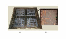
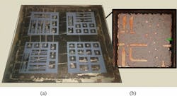
Integrated SoC WLAN receivers may suffer from very-low quality factors (Qs). As a result, using separate components for low-noise-amplifiers (LNAs) and bandpass filters (BPFs) could increase the performance of a receiver while decreasing its size. To keep a low footprint, the researchers used a low-loss organic substrate, ZEONIF XL (X-L). Two designs were run with 3D EM simulation software for optimization purposes—a package with an LNA and integrated BPF and one without the BPF, which proved the design techniques increased performance.
The overall thickness of the WLAN Rx module is 160 μm in a footprint measuring 5.5 × 2.0 mm. With a low pass-band insertion loss of 2.3 dB, the BPF operates well with 15 dB of return loss. The peak gain of the device is 11 dB with greater than 30 dB of attenuation in the adjacent bands. Considering a comparable wire-bonded, LNA-equipped WLAN receiver, the researchers claim their design is less than 1.5 times smaller (including the bandpass filter). See “Ultraminiaturized WLAN RF Receiver Module in Thin Organic Substrate,” IEEE Transactions on Components, Packaging and Manufacturing Technology, Aug. 2014, p. 1276-1283.
About the Author
Jean-Jacques DeLisle
Jean-Jacques graduated from the Rochester Institute of Technology, where he completed his Master of Science in Electrical Engineering. In his studies, Jean-Jacques focused on Control Systems Design, Mixed-Signal IC Design, and RF Design. His research focus was in smart-sensor platform design for RF connector applications for the telecommunications industry. During his research, Jean-Jacques developed a passion for the field of RF/microwaves and expanded his knowledge by doing R&D for the telecommunications industry.
