DDS Model Tunes Doppler Simulation
This file type includes high resolution graphics and schematics when applicable.
Testing satellite navigation receivers usually depends on signal simulation to evaluate a satellite-communications (sitcom) receiver under high-dynamic-range conditions.1-3 A third-order direct-digital synthesizer (DDS) is invaluable for such simulation and testing, and the accumulation clock rate for each of the three DDS stages can either be the same or different. Numerous reports have been based on the use of same-clock conditions for these multiple-stage DDS sources,4-6 with few studies of higher-order, hybrid-clock DDS sources, structured with multiple cascade accumulators with different accumulation clock rates.7
Related Articles
• eLTE-Based Railway Solution Covers 400 MHz to 5.8 GHz
• Microwave Diodes… Why a Schottky-barrier? Why a Point-contact?
• Sea Radar System Detects Moving Targets While Avoiding Clutter
To better understand these hybrid-clock, third-order DDS sources, a simulation model was developed and an output phase expression for the model was derived. By analyzing this model, it will be shown that hybrid and same-clock higher-order DDS sources can be combined and their models unified. Simulation results for the model will show that it can be used for high-precision Doppler simulation, and that the hybrid clock operation can greatly reduce power consumption compared to same-clock higher-order DDS operation.
The function of a DDS accumulator can be expressed as a simple relationship (Eq. 1), where the output of the DDS accumulator is represented as acc(n), with n as the clock number index, n0 as the clock number when the accumulator resets, x as the initial value, and k as the accumulation step.6 When the DDS accumulator is implemented in a field-programmable gate array (FPGA), the output always lags behind the input by one clock cycle.
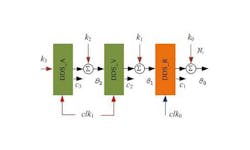
Figure 1 shows a third-order, hybrid-clock DDS model, with three cascaded DDS accumulators. The first-stage accumulator is running at a different accumulation clock rate than the other two accumulators. The three accumulators in this hybrid-clock model are defined as the acceleration DDS accumulator (DDS_A), the velocity DDS accumulator (DDS_V), and the phase DDS accumulator (DDS_R), respectively.
Parameters k0 through k3 are the initial accumulation parameters of each accumulator stage; parameters θ0 through θ2 are the outputs of each different accumulator stage; N0 is the word length of parameter k0; and c1 through c3 are the bits that must be truncated when adding the accumulator output to the initial accumulator parameter. Parameters clk0 and clk1 are clock signals driving the first and additional accumulator stages, respectively, as represented in Eq. 2.
In Eq. 2, the clock frequency division coefficient, W ≥ 1, is an integer, so that the clock rate clk0 will be at integral multiples of clk1. If clk0 < clk1, the influence of the latter two accumulators on the first-stage accumulator can be converted and equivalent to a DDS model with same-clock accumulators. In the case of W = 1, the DDS model degenerates into the same-clock model presented in ref. 6.
Based on the model of Fig. 1, the output of each accumulator stage is derived when W is an unknown parameter. For DDS_A, when its initial value is k2, the step value is k3, and the number of the accumulated clock is m, so that its corresponding output sequence can be obtained according to Eq. 3.
Similarly, when the initial value for DDS_V is k1, the step is θ2(m - 1), and it is possible to calculate the corresponding output sequence by means of Eq. 4:
For the output sequence of DDS_R, while its initial value is k0, the step is θ1(n - 1), and the number of the accumulation clock is n; its output sequence can be expressed as Eq. 5. But since W is an unknown, the right-hand side of Eq. 5 cannot be directly expanded and summed:
Supposing that Y = [n/W], where the square brackets denote rounding the contained value to an integer, it is then possible to perform the summation of Eq. 6:
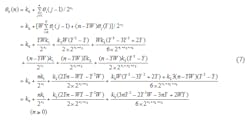
Incorporating Eq. 6 into Eq. 5 results in Eq. 7:
This file type includes high resolution graphics and schematics when applicable.
Applying The DDS
This file type includes high resolution graphics and schematics when applicable.
To apply the hybrid-clock third-order DDS to realize a high-precision simulation of satellite navigation signal Doppler frequency shift, it is necessary to obtain the initial accumulation parameters (k0 through k3), as well as to restrict the word-length parameters (N0, c1 through c3) in the corresponding simulation model.
For the satellite navigation signal simulator, the simulated signal Doppler is generated due to radial variable motion between the receiver and satellite. Assuming that pseudorange between the receiver and satellite is R at a moment t = 0, the relationship of parameters in the model describing such radial motion must satisfy the conditions presented in Eq. 8.3,8
where:
t = the run duration;
v(t) = the real-time radial velocity;
s(t) = the real-time radial pseudorange amount;
R = the initial pseudorange amount;
v = the initial velocity;
a = the accelerated velocity; and
â = the amount of jerk.
The received signal Doppler frequency shift can be expressed as Eq. 9:
where:
fd(t) = the Doppler frequency shift;
fT = the nominal frequency of the simulated signal; and
c = the speed of light.
The signal phase can be expressed as Eq. 10:
If the signal phase is made discrete in Eq. 10, the sample clock is the working clock of the first-stage phase accumulator. When the clock cycle period is Tc = 1/fc, the discrete signal phase sequence can be expressed by Eq. 11:
The final output phase of the hybrid-clock third-order DDS should precisely correspond to the simulated signal phase. To obtain initial accumulation parameters k0 through k3), it can be presumed that the output phase of the third-order DDS satisfies Eq. 12 at n = 0, W, 2W…iW for I ∈ Z+:
If Eq. 12 is the constraint condition, and N0 and c0 through c3 are treated as known parameters, the values of k0 through k3 in Eq. 7 can be obtained. In the case where n = 0, W, 2W, 3W, from Eq. 12, Eq. 13 can be obtained:
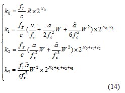
A set of solutions from Eq. 13 can be obtained resulting in Eq. 14:
To prove that Eq. 14 satisfies Eq. 12 at any i ∈ Z+, mathematical induction is applied, with the following steps. For step 1, because Eq. 14 satisfies Eq. 12 when i = 0, 1, 2, and 3, it will satisfy the first step of the mathematical inductor. For step 2, supposing that Eq. 14 satisfies Eq. 12 when i = j, then when i = j + 1, it will yield Eq. 15:
Introducing Eq. 14 into Eq. 15 yields Eq. 16:
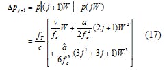
Similarly, the difference between p(jW) and p[(j + 1)W] can be expressed as Eq. 17:
Equation 18 can be obtained from Eqs. 16 and 17:
From Eq. 18, it is clear that Eq. 14 satisfies Eq. 12 when i = j + 1, which guarantees the validity of Eq. 14 for all i ∈ Z+ satisfying Eq. 12.
Compared with the results of ref. 6, the calculation results of same-clock condition is the case of W = 1 in Eq. 14. When W > 1, within each clk1 clock cycle period, the third-order DDS runs like a first-order DDS. Therefore, the hybrid-clock third-order DDS will generate larger pseudorange error as a same-clock DDS while running with the initial accumulation parameters calculated based on Eq. 14. Ignoring word-length quantization errors, this error can be expressed as Eq. 19:
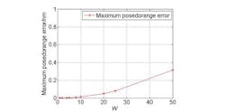
Analysis of Eq. 19 is relatively complex, so the simulation method can be used to analyze the error. In case of fc = 100 MHz and W ≤ 50, and assuming the conditions of Eq. 2 are met, the third-order DDS output pseudorange errors under the high-dynamic-range conditions represented by v = 1000 m/s; a = 1000 m/s2, and â = 1000 m/s3 will be simulated. For a third-order DDS simulation run time of 10 ms, the maximum pseudorange errors for different W values are shown in Fig. 2. As W increases, the maximum pseudorange error caused by the hybrid clock increases correspondingly. In the case of W ≤ 10, the maximum pseudorange error is smaller than 10-10 m.
If fc/W is large enough, the influence of the initial accumulation parameters on the Doppler frequency shift simulation errors under hybrid clock conditions can be ignored. With currently available FPGA-based DDS instruments, such a conditions can easily be satisfied.
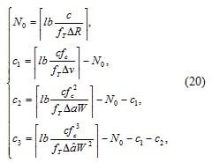
Doppler simulation errors for the hybrid-clock third-order DDS can be mainly attributed to the quantization error of the word length at each stage. To achieve the required resolution for an accurate simulation, the word length of each accumulator stage must be designed. For this analysis, suppose that ΔR, Δv, Δa, and Δâ are the resolution of the pseudorange, the velocity, the acceleration, and the jerk amount, respectively. Fr the case of ki = 1, the corresponding parameter should be smaller than the resolution. The word length obtained from Eq. 14 can be expressed in terms of Eq. 20:
The square brackets in Eq. 20 represent rounding to an integer value. It should be evident from Eq. 20 that the word length parameters for all three accumulators are N0 + c1, N0 + c1 + C2, and N0 + c1 + c2 + c3, respectively. In addition, all the word length parameters are restricted to the lower bounds; in order to increase simulation precision, the word length parameter must be increased appropriately.
When W = 1, Eq. 20 reverts to the results for a same-clock third-order DDS. Considering the initial accumulation parameter calculation expressions, it is clear that the same-clock third-order DDS simulation model can be unified with the hybrid-clock simulation model. Under the requirement of the same design resolution, the lower bound of word length calculated by Eq. 20 is associated with W. The results obtained when W > 1 is shorter than the one when W = 1. Therefore, the resource and static power consumption can be reduced.
This file type includes high resolution graphics and schematics when applicable.
A Closer Look
This file type includes high resolution graphics and schematics when applicable.
Using a 1561.098-MHz BeiDou2 B1 carrier signal simulation as an example,9 the reductions in word length can be analyzed while W > 1. For this example, the sampling frequency is assumed to be 100 MHz, the clock frequency division coefficient W can be 1 or 10, and the resolutions of the pseudorange, velocity, acceleration, and jerk variables are set to ΔR = 5 cm, Δv = 1 mm/s, Δa = 10 mm/s2, and Δâ = 10 mm/s3. The word length of each DDS stage can be obtained from Eq. 20 while W = 1 and W = 10. The values of N0 = 2 and c1 = 33 do not matter whether W = 1 or 10. For c2 = 23 and c3 = 26 when W = 1 and c2 = 20 and c3 = 23 when W = 10, three bits of resolution are reduced at each DDS stage.
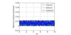
The model was used to simulate the performance of a hybrid-clock third-order DDS. Simulation parameters were similar to those used previously, with W = 10, and with word-length parameters of N0 = 6, c1 = 33, and c2 = 23. With an initial velocity of 0, the acceleration is 0 m/s2, and the jerk rates are 100 m/s3, 500 m/s3, and 1000 m/s3, respectively. To avoid errors from a long accumulation period, caused by DDS word-length quantization, the hybrid-clock, third-order DDS is initialized every other 10 ms during simulation. The maximum phase error for the DDS accumulator occurs at every 10-ms simulation interval. Under different jerk amounts, the maximum phase error is always less than 0.02 mrad (Fig. 3).
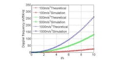
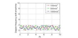
During this simulation, the phase sequence of the DDS_R accumulator within each simulation interval is obtained; a direct phase modeling method was adopted to estimate the Doppler frequency shift produced.10 By adopting this method, the frequency estimation accuracy is no longer dominated by receiver Doppler measurement accuracy when the receiver is adopted for verification. The simulation results are shown in Fig. 4 and the corresponding Doppler frequency shift errors in Fig. 5.
To check the accuracy of the Doppler frequency-shift estimations during the simulation, the data sampling intervals in Figs. 4 and 5 were increased to 200 ms. As Fig. 5 shows, even under different jerk rates, the hybrid-clock third-order DDS can maintain high Doppler simulation accuracy, and the error is always less than 2 mHz. The table compares resource and power consumption results for cases of W = 1 and W = 10.
To compare the simulation results to an actual unit, the FPGA used for analysis in the table was a model XC6SLX150 from Xilinx, and the power consumption analysis was produced with the aid of the company’s XPower Analyzer. In the case of W > 1, the resource and power consumption of the third-order DDS are decreased compared to a situation using multiple similar clocks. For W = 10, the word length reduction of each of the latter two accumulators is only 3, so the reduction of the resource and static power consumption is not obvious. However, the accumulation clock rate of the last two DDS accumulator stages is reduced to 1/W of the same-clock condition, which results in a dynamic power consumption reduction of approximately 1/W.
This hybrid-clock third-order DDS model can be used under both same-clock and hybrid-clock DDS conditions. The simulation results for the BeiDou2 B1 carrier signal show that the signal Doppler simulation method achieves precision of 2 mHz. Compared with the same-clock condition, the third-order DDS under hybrid-clock conditions operates with less resource requirements and power consumption. This simulation approach provides a means of precisely simulating Doppler signals, and is particularly useful for modeling portable high-dynamic-range satellite navigation equipment.
Zhang Yin, Doctoral Candidate
Li-Cai-Hua, Assistant
Huang Yang-Bo, Assistant
Zhang Guo-Zhu, Associate Professor
Ou Gang, ProfessorCollege of Electronic Science and Engineering, National University of Defense Technology, Changsha 410073, People’s Republic of China
This file type includes high resolution graphics and schematics when applicable.
References
This file type includes high resolution graphics and schematics when applicable.
1. D.U. Lee, W. Luk, and J.D. Villasenor, “A Gaussian noise generator for hardware-based simulations,” IEEE Journal of Transactions on Computers, 2004, Vol. 53, No. 12, 2004, pp. 1523-1534.
2. A. Brown and N. Gerein, “Modeling and simulation of GPS using software signal generation and digital signal reconstruction,” Proceedings of the ION National Technical Meeting, 2000, pp. 646-652.
3. Wei Qi, Qing Chang, and Qishan Zhang, ”Arithmetic of Doppler simulation in high dynamic signal simulator,” Acta Aeronautica ET Astronautica Sinica, Vol. 29, No. 5, 2008, pp. 1252-1257.
4. Yang Xiang and Xiulin Hu, ”Key Technique for an IF Signal Simulator in High Dynamic GPS,” Journal of Huazhong University of Science & Technology (Natural Science), Vol. 37, No. 12, 2009, pp. 9-12.
Related Articles
• eLTE-Based Railway Solution Covers 400 MHz to 5.8 GHz
• Microwave Diodes… Why a Schottky-barrier? Why a Point-contact?
• Sea Radar System Detects Moving Targets While Avoiding Clutter
5. Bo Zhang, Guangbin Liu, and Wei Jiao, “High-order DDFS Applied in Simulated High-dynamic GNSS signal synthesis,” Proceeding of the 9th International Conference on Electronic Measurement and Instruments, Beijing, China, IEEE Computer Society, 2009, pp. 4102-4106.
6. Yuanyuan Song, Hui Zhou, Tao Zeng, and Lei Zhang,” Algorithm and Realization of High Dynamic Satellite Signal Doppler Simulation Based on FPGA,” Proceedings of the ION National Technical Meeting, 2010, pp. 1044-1050.
7. Xuejuan Zhou and Liqiao Dong, “A New Method for High-Precision Dynamic Clock in Navigation Simulator,” Journal of Radio Engineering, Vol. 41, No. 11, 2011, pp. 37-39.
8. Chengjun Li, Mingquan Lu, and Zhengming Feng, ”Mathematical model and realization for GPS IF Signal Simulator,” Journal of Tsinghua University (Science and Technology), Vol. 48, No. 10, 2008. pp. 1582-1585.
9. Dou Bei, “Navigation Satellite System Signal In Space Interface Control Doucment,” China Satellite Navigation Office, 2012.
10. Mingjian Chen, Chunsheng Liu, and Xiu Wang, “Application of Phase Modeling Method and Smooth Phase Difference Method to Instantaneous Frequency Estimation,” Shipboard Electronic Countermeasures, Vol. 31, No. 12, 2008, pp. 73-77.
This file type includes high resolution graphics and schematics when applicable.
