Phased Array Antenna Receives 4G Networks
This file type includes high resolution graphics and schematics when applicable.
Fourth-generation (4G) cellular networks rely on many key components to provide the bandwidth and coverage that wireless service providers and their customers expect. One of these components is a phased-array antenna system with beam-steering capabilities that supports communications between relay stations and base stations. The proposed antenna design operates at 3.42 GHz and features 21.17 dBi gain and 424 MHz bandwidth, employing a least-mean-square (LMS) algorithm to provide a steerable mainlobe response with desired nulls and sidelobe suppression.
Phased-array antennas have been used in a wide range of applications, from military systems to commercial cellular communications networks. They are often used in wireless systems to steer signals from base stations to desired destinations while creating nulls to suppress interference.1,2 A number of algorithms have been developed and proposed for beam-steering purposes, including LMS, the constant modulus algorithm (CMA), and the recursive least-squares (RLS) algorithm.3,4 These algorithms are characterized by different complexity levels and convergence times.5,6 In addition, a wide range of antenna shapes and configurations have been proposed for use in phase-array systems for achieving bandwidth and gain enhancements.7,8
The proposed phased-array system was developed for use in a prototype WiMAX relay station9 to establish a backhaul link between a relay station and base station. It includes a 4 x 4 microstrip-based modified E-shaped patch array10 based on a stacked geometry.11 In addition, a beam-forming circuit was designed and fabricated for power division, signal processing, and array excitation. An LMS algorithm was used to properly assign phases and amplitudes to each radiating element and thus steer the radiation mainlobe to a base station.
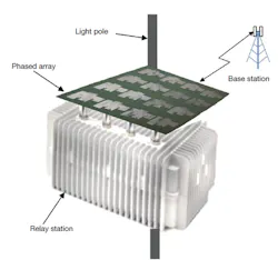
Version 14 of the Mathcad simulation software from Parametric Technology Corp. was used to generate the LMS algorithm. When the required element phases and amplitudes are obtained, they are applied to the array simulations as well as to the fabricated prototype to derive simulated and actual radiation patterns. Figure 1 shows the application of the proposed phase-array antenna design.
1. The proposed phased-array-antenna system can be used to connect cellular relay stations to 4G base stations.
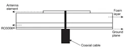
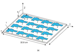
Figure 2 shows the dimensions for the 4 x 4 antenna array. The modified E-shaped elements are placed on a foam substrate with relative dielectric constant (εr = 1) with height, h, of 0.5 cm. The foam substrate is then placed on RO3006 circuit-board material from Rogers Corp. with εr = 6.15 and h = 1.28 mm. Next, the RO3006 substrate is mounted on a ground plane of 35-μmm-thick copper. Figure 3 shows the structure of the array, in which the modified E-shaped elements are coaxial fed. The two circuit substrates are used for enhanced bandwidth and gain.10Figure 4(a) depicts the phased array for simulation purposes, while Fig. 4(b) shows the fabricated array.
2. The phased-array antenna uses an E-shaped configuration to achieve high gain.
3. This cross-sectional view shows how a foam layer is used with a commercial circuit-board layer in the antenna design.
4. The phased-array antenna design was evaluated in terms of (a) software simulations and by means of measurements of a fabricated design (b) in an anechoic chamber.
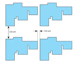
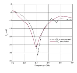
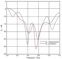
Figure 5 denotes the edge-to-edge distance between elements. The center-to-center distance between two adjacent elements is 0.8λ0, where λ0 is the free-space wavelength. This value was chosen to produce a radiation pattern with low sidelobe levels and to prevent grating lobes.12Figure 6 provides the simulated and measured S11 response for element “1” in Fig. 4(a). For the experimental S11 measurements of element 1, all other elements are terminated using 50-Ω impedance to eliminate mutual coupling effects.
5. This diagram shows the inter-element spacing in the 4 x 4 antenna array.
6. These plots compare the simulated and measured S11 responses for the E-shaped antenna.
The two S11 curves of Fig. 6 are in close agreement, verifying that the proposed antenna array operates at 3.418 GHz with bandwidth of 424 MHz (S11 < -10 dB) or 12.4%. The S11 measurements were obtained using a model MS2036A vector network analyzer (VNA) from Anritsu Co.
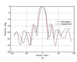
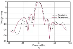
Figure 7 offers simulated and measured radiation patterns [for the θ angle and XYZ planes denoted in Fig. 4(a)] for the 16-element array, with measurements performed in an anechoic chamber. The currents that excite each radiation element have the same amplitude and phase. The radiation pattern that results has a mainlobe at θ = 0 deg. and sidelobe levels of less than 10 dBi. The radiation patterns depicted in Fig. 7 were obtained at 3.418 GHz.
7. These radiation patterns are shown in terms of θ for (a) φ = 0 deg. (in the XZ plane) and (b) φ = 90 deg. (in the YZ plane).
The table compares the proposed array with a commercial antenna at 3.5 GHz in terms of gain, bandwidth, and half-power beamwidth (HPBW) in the YZ and XZ planes. The array’s enhanced gain and low HPBW are suitable for use in point-to-point communications applications. The array satisfies the requirements of the IEEE 802.16j protocol for WiMAX, and can be used for achieving a backhaul link between a relay station and a base station.
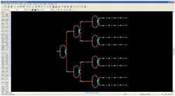
The beam-forming module is a planar design with two substrates, including two eight-way power dividers. It was simulated and optimized with the help of the Advanced Design System (ADS2009) simulation software from Agilent Technologies and then fabricated. It includes Wilkinson power dividers,13 100-Ω chip resistors, commercial digital attenuators (model HMC629LP4 from Hittite Microwave Corp.), and digital phase shifters (model HMC648LP6 from Hittite). The microstrip circuit was fabricated on RO4003 circuit-board material from Rogers Corp. with relative permittivity of 3.55 and thickness of 0.508 mm. A second RO4003 board is placed beneath the first substrate, on the top of which the ground plane is positioned.
8. The two photographs shows the top view (a) and bottom view (b) of the beam-forming unit, while the cross-sectional diagram (c) shows the stacked circuit substrates.
The amplitudes and phases of each radiating element are produced as a result of digital inputs; the resulting signal amplitudes and phases are assigned to specific attenuators and phase shifters, respectively. Figure 8(c) provides a cross-sectional view of the proposed beam-forming circuit, with the two substrates held together via holes. The length of the microstrip line on the top part of the circuit is an integer multiple of λ0(f0 = 3.5 GHz), while the width is defined using the formula in ref. 14. Figure 9 shows the layout of the beam-forming circuit design. The simulated and measured S11 performance of the beam-forming circuit is shown in Fig. 10.
9. This layout shows the microstrip circuit pattern for the beam-forming module.
10. This plot shows the simulated and measured S11 responses for the eight-way Wilkinson power divider.
The S11 measurements on the circuit were performed with the Anritsu MS2036A VNA. The beam-forming circuit operates from 3.3 to 4.0 GHz, a 700-MHz bandwidth with S11 less than -10 dB. The minimum experimental value of S11 is -27.112 dB at 3.38 GHz. As Fig. 10 shows, the measured and simulated responses are in good agreement, with differences resulting from ohmic, dielectric, and conductor losses in addition to microstrip line coupling. The beam-forming network thus covers the frequency range of the antenna array developed previously, making it a good match for the combined design. Figure 11 shows the antenna array together with the beam-forming circuit.
11. This diagram shows how test signals were created for evaluating the phased-array antenna system.
The test signals are generated by a model MXG N5182A commercial signal generator from Agilent Technologies. They are guided to a commercial two-way SMA power divider with frequency range of DC to 18 GHz, which splits the test signals into two equal outputs. These signals are then sent to the beam-forming module. Within the module, the test signals are further divided into 16 microstrip lines which feed each of the 16 antenna array elements. Commercial phase shifters and attenuators are incorporated to achieve the desired radiation pattern. The beam-forming circuit and the array are connected through SMA cables. In addition, the power divider is connected to the beam-forming circuit via SMA cables. All measurements are performed in an anechoic chamber.
The antenna array’s radiation pattern can be shaped through the application of the LMS algorithm.15 It is a gradient-based algorithm which performs iterative operations to minimize the mean square error between the array output and a reference signal. The algorithm was developed and operates according to Version 14 of the Mathcad software. A set of requirements is first defined regarding radiation pattern shape. The algorithm is then executed to yield the amplitude and phase for each patch element to create the required radiation pattern.
Three beam-forming scenarios were considered for the proposed design. In the first scenario, the conditions included a maximum level at (-18 deg., 0 deg.), a null at (34 deg., 0 deg.) and sidelobe level (SLL) of less than -10 dB. The specific quantized values of amplitude and phase17,18 required for this scenario are:
α = [0,-3,-6,-9,-12,-15,18,-21,-24,-27,-30,-33,-36,-39,-42,-45] in dB
and
β = [0, 5.625, 11.250… 354.375] in deg. with step of 5.625 deg.
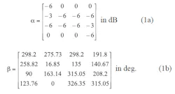
The algorithm gives the following results in terms of amplitude and phase:
These results are assigned to each radiating element for the purpose of measurements and simulations, with the simulated and experimental radiation patterns for the phased array in this scenario shown in Fig. 12. The requirements of the scenario have been met. The sidelobe levels on both curves are less than -10 dB. The null angle is 34 deg., while the angle of maximum response is -18 deg. The deviations in the experimental results can be attributed to ohmic, dielectric, and conductor losses; line coupling; and imbalance phenomena of the attenuators and phase shifters. Imbalance phenomena are relevant to errors in attenuation and phase assignment to excitation currents due to circuit losses. In spite of these imbalances and losses, the radiation pattern exhibits the desired form.
12. These curves show the simulated and measured radiation patterns for the phased-array antenna system in the first scenario.
In the second scenario, the maximum is at (22 deg., 0 deg.), the null is at (80 deg., 0 deg.), and the SLL is less than -10 dB. The procedure used in the first scenario is followed, with the LMS algorithm yielding the following results:
The simulated and experimental response curves for this scenario are shown in Fig. 13. The simulation response meets the requirements except for the maximum of the mainlobe, where the simulation curve presents θmax = 20 deg. The measured response shows the mainlobe maximum at θmax = 18 deg. This deviation may be the result of power divider and cable losses in the experimental setup.
13. These curves show the simulated and measured radiation patterns for the phased-array antenna system in the second scenario.
In the third scenario, the maximum is at (-24 deg., 0 deg.), the null is at (20 deg., 0 deg.), and the SLL is less than -10 dB. For this scenario, the LMS algorithm yields the following results:
In this case the curves produced by simulation and experiment satisfy the requirements set by the scenario (Fig. 14). Blue and green lines coincide at high degree. The differences between simulation and experiment are probably caused by power-distribution losses in the beam-forming circuit.
14. These curves show the simulated and measured radiation patterns for the phased-array antenna system in the third scenario.
In summary, the simulated and measured results for the phased-array antenna system and its beam-forming network were in close agreement in most cases. The phased-array module—a compact 4 x 4 array with better than 21dBi gain across a 424MHz bandwidth at 3.5 GHz—was designed and simulated with the aid of the HFSS (Version 11) electromagnetic (EM) simulation software from Ansys. The proposed array was compared to a commercial array, revealing that it exhibits higher gain over a narrower beamwidth.
Ioannis Petropoulos
Research Assistant, PhD Candidate, Wireless Communication and e-Applications Research Group, Department of Electronics, Technological Educational Institute of Athens, Athens, Greece; 00302105385367, FAX: 2105385304, e-mail: [email protected].
Nikos Athanasopoulos
Temporary Lecturer, Department of Electronics, Technological Educational Institute of Athens, Athens, Greece; 00302105385367, FAX: 2105385304, e-mail: [email protected].
Konstantinos Voudouris
Associate Professor on Wireless Telecommunications Systems, Department of Electronics, Technological Educational Institute of Athens, Athens, Greece; 00302105385367, FAX: 2105385304, e-mail: kvoud@teiath.gr.
Raed A. Abd-Alhameed
Professor of Electromagnetics and Radio Frequency Engineering, School of Engineering, Design, and Technology, University of Bradford, Richmond Road, Bradford, BD7 1DP, United Kingdom; (+44) (0) 1274 23 4542, e-mail: [email protected].
Steve M.R. Jones
Lecturer in Electronics and Telecommunications, School of Engineering, Design, and Technology, University of Bradford, Richmond Road, Bradford, BD7 1DP, United Kingdom; (+44) (0) 1274 23 4542, e-mail: [email protected].
References
1. Lal C. Godara, “Application of Antenna Arrays to Mobile Communications,” Proceeding of the IEEE, Vol. 85, No. 8, August 1997, pp. 1195-1234.
2. Salvatore Bellofiore, Jeffrey Foutz, Constantine A. Balanis, and Andreas S. Spanias, “Smart-Antenna System for Mobile Communication Networks Part 2: Beamforming and Network Throughput,” IEEE Antennas and Propagation Magazine, Vol. 44, No. 4, August 2002.
3. S. Das, “Smart antenna design for wireless communication using adaptive beam-forming approach,” TENCON 2008 - 2008 IEEE Region 10 Conference, November 19-21, 2008, pp. 1-5.
4. Reeta Gaokar and Dr. Alice Cheeran, “Performance Analysis of Beamforming Algorithms,” International Journal of Electronics & Communication Technology, Vol 2, No. 1, 2011.
5. Y.H. Chen, Jun-Horng Chen, Peng Chia Hsien, Dau-Chyrh Chang, and Jung-Hao Huang, “Performance evaluation of mobile WiMAX beam forming network implemented by RF digital step attenuators,” 14th European Wireless Conference, June 22-25, 2008, pp. 1-6.
6. J.M. Samhan, R.M. Shubair, and M.A. Al-Qutayri, “Design and Implementation of an Adaptive Smart Antenna System,” Innovations in Information Technology, November 2006, pp. 1-4.
7. Kainan Zhao, Fei Liu, Wenhua Chen, and Zhenghe Feng, “Bandwidth-enhanced design of a planar switched parasitic array antenna,” 2010 International Conference on Microwave and Millimeter Wave Technology (ICMMT), May 8-11, 2010, pp. 1129-1131.
8. Qinjiang Rao and T.A. Denidini, “Electromagnetically coupling fed broadband low profile microstrip antenna array,” 2007 IEEE Antennas and Propagation Society International Symposium, June 9-15, 2007, pp. 893-896.
9. V. Genc, S. Murphy, Y. Yu, and J. Murphy, “IEEE 802.16j Relay-based Wireless Access Networks: An Overview,” IEEE Wireless Communications Magazine, Special Issue on Recent Advances and Evolution of WLAN and WMAN Standards, 2008.
10. A.C.O. Pedra, G. Bulla, P. Serafin, C.R. Fernandez, G. Monser, and A.A.A. de Salles, “Bandwidth and size optimization of a wide-band E-shaped patch antenna,” SBMO/IEEE MTT-S International Microwave and Optoelectronics Conference, IMOC 2007., October 29 to November 1 2007, pp. 422-426.
11. D. Yoharaaj, D. Azmir, Raja Syamsul, and Ismail, Alyani, “A New Approach for Bandwidth Enhancement Technique in Microstrip Antenna for Wireless Applications,” RF and Microwave Conference, September 2006, pp. 205-209.
12. R. Jedlicka, M. Poe, and K. Carver, “Measured mutual coupling between microstrip antennas,” IEEE Transactions on Antennas & Propagation, Vol. 29, No. 1, January 1981, pp. 147-149.
13. E.J. Wilkinson, “An N-way hybrid power divider,” IRE Transactions on Microwave Theory & Techniques, Vol. 8, January 1960, pp. 116-118.
14. E.O. Hammerstad, “Equations for microstrip circuit design,” in Proceedings of the 5th European Microwave Conference, Hamburg, Germany, September 1975, pp. 268-272.
15. Qun Yang, Xiang-yu Cao, Yao Xu, and Xiao-fei Xu, “Performance of LMS algorithm in smart antenna,” 2010 International Conference on Microwave and Millimeter Wave Technology (ICMMT), May 8-11, 2010, pp. 1372-1375.
16. C.A. Balanis, Antenna Theory: Analysis and Design, Wiley, New York, 1997.
17. Data sheet for model HMC629LP4, Hittite Microwave Corp., Chelmsford, MA, 2008, www.hittite.com.
18. Data sheet for model HMC648LP6, Hittite Microwave Corp., Chelmsford, MA, 2008, www.hittite.com.
This file type includes high resolution graphics and schematics when applicable.
