QPSK Modulator Transmits Satcom Data
This file type includes high resolution graphics and schematics.
Digital modulation is often a means of transmitting payload data from orbiting satellites to ground stations. Such is the case for satellites in the Indian Remote Sensing (IRS) satellite system. In one such approach, quadrature phase-shift-keying (QPSK) modulation provides both spectral and power efficiency. In a QPSK modulator, two data streams simultaneously modulate a carrier signal. For optimum use of available satellite power, an unbalanced QPSK (UQPSK) modulator is often used. The design and simulation for such a modulator will be shown here, along with methods for demodulating such signals.
Communications channels in satellite-communications (satcom) systems, as well as communications systems in general, can be categorized as being power- or bandwidth-limited. For power-limited communications channels, coding schemes are typically applied to save power at the expense of bandwidth. In bandwidth-limited channels, spectrally efficient modulation schemes are often used to conserve bandwidth. The prime goal of spectrally efficient modulation is to optimize bandwidth efficiency, which is defined as the ratio of the data rate to the channel bandwidth (in b/s/Hz). A secondary goal of such a modulation scheme is to achieve high bandwidth efficiency with minimum signal power.
QPSK modulation results in optimum use of both spectrum and power when the data rates for the two channels—or the in-phase (I) and quadrature (Q) signal components—are the same. But when two data streams atdifferent bit rates from two independent payloads must be transmitted, the normal procedure of formatting the data for modulation onto the carrier becomes very complicated. The easiest way is to transmit the two different data streams on the two QPSK channels by direct modulation, which results in the two channels of the modulator having different data rates. The higher of the data rates determines the bandwidth required for the modulated carrier and the transmitter output power will be equally shared by the two different data streams.
To optimize available transmit power from a satcom system, an UQPSK modulator is proposed here, where the power level of the low-data-rate channel can be reduced to achieve the same carrier-to-noise (Eb/No) ratio for both channels. This can be achieved by unbalancing the amplitudes of the carrier’s signal components in the I and Q channels of a conventional QPSK modulator. The amplifier power following the modulator is shared between the I and Q channels in proportion to the amplitudes of the I and Q signal components of the modulated carrier.
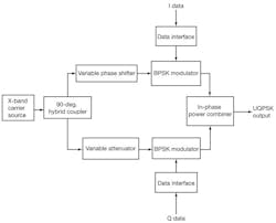
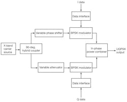
Figure 1 shows a block diagram of the proposed UQPSK modulator. In a conventional QPSK modulator, the carrier source signal is divided equally by a 3-dB/90-deg. branch line hybrid coupler to yield two equal-amplitude carriers in quadrature. Both carriers are modulated with I and Q data streams using binary-phase-shift-keying (BPSK)modulation. The BPSK-modulated carriers are combined in an in-phase Wilkinson power combiner to produce a QPSK-modulated carrier. When data of different bit rates are to be modulated, an UQPSK modulator can be used.
1. This block diagram represents the proposed UQPSK modulator.
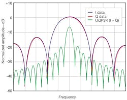
In the case of an UQPSK modulator, for optimum utilization of power, an attenuator is added to the low-data-rate channel to reduce the power. A phase shifter is added tothe high-data-rate channel to compensate for the phase shift introduced by the attenuator in the low-data-rate channel. The resulting output isa UQPSK-modulated signal. The mainlobe bandwidth will be determined by the high-data-rate channel. Figure 2 shows a plot of the I and Q data, along with the simulated UQPSK spectrum.
2. Figure 2 shows the I and Q data along with the simulated UQPSK spectrum.
The UQPSK modulator was realizedusing a 3-dB/90-deg.branch line coupler, two double-balanced mixers, a phase shifter, an attenuator, and an in-phase power combiner. A dielectric resonator oscillator (DRO), generating a carrier signal at 8725 MHz,served as the carrier source for the modulator. For demonstration purposes, 200- and 50-kb/s pulse streams were used to modulate the carrier signal. A data generator providing different bit rates (other than these two rates) was not readily available. The use of two different data generators would require that data to be synchronized with a clock.
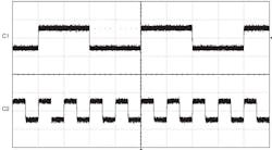
In this experiment, the two data streams were generated from a single generator. Data at 200kb/s was taken from the generator and divided by four using JK flip-flops to generate the 50-kb/s data. The two data streams of unipolar format were converted to bipolar format using a transistor-level converter circuit. The I data and derived Q data are shown in Fig. 3. The data streams were fed to the UQPSK modulator.
3. The I and Q data schemes are shown for feed to the UQPSK modulator.
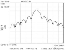
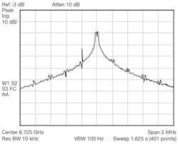
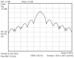
The carrier was fed to a 3-dB/90-deg.hybrid coupler,which generates two carriers of equal amplitude and 90-deg.phase differencefor the modulator’s I and Q channels.The data rate of the Q channel is one-fourth the data rate of the I channel. As a result, the power in the Q channel should be reduced proportionally to one-fourth the level of the power in the I channel. This is accomplished by means of 6-dB attenuation in the Q channel. To compensate for the phase shift introduced by the attenuator, a phase shifter was added to the I channel. These two carrier signals were then modulated by the I and Q data using double-balanced mixers [a model DML-2B-10G mixer from Merrimac Industries]. Those modulated spectra are shown in Figs. 4 and 5, respectively. The BPSK modulated signals were fed to an in-phase power combiner to produce the UQPSK modulated output shown in Fig.6.
4. The modulated spectra for the I data are shown here.
5. The modulated spectra for the Q data are shown here.
6. BPSK modulated signals were fed to an in-phase power combiner to produce a UQPSK-modulated output.
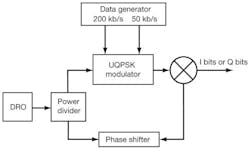
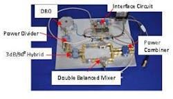
Figure 7 shows a block diagram of the modulator/demodulator test setup, while Fig. 8 features a photograph of the test setup. Since there was no standard UQPSK demodulator equipment available at the workplace, the modulated data was recovered as shown in Fig. 7.
7. This block diagram details the different functions contained in the modulator/demodulator test setup.
8. This photograph shows the actual modulator/demodulator test setup.
To produce two carrier outputs from the DRO, a power-divider module was used. One of the power-divider’s outputs was fed as an input to the UQPSK modulator. The UQPSK-modulated output and the other DRO carrier output from the power divider were fed to a mixer (not shown in Fig. 8) to bring back the original modulated data. A variable phase shifter (not shown in Fig. 8) was used in the carrier path. When the carrier phase was synchronized with the I channel carrier of the UQPSK signal, the I data stream was demodulated. When the phase of the carrier was shifted by 90 deg. using the variable phase shifter, the Q data stream was demodulated. Thus, by varying the phase of the phase shifter, the I and Q data streams could be demodulated; the resulting waveforms of that process are shown in Figs. 9 and 10.
9. Demodulated I channel data was achieved with the help of a phase shifter.
10. Demodulated Q channel data was achieved with the help of a phase shifter.
In summary, an unbalanced QPSK modulator was demonstrated; it is a variant of a standard QPSK modulator. This unbalanced QPSK modulator is useful for transmitting different (unequal) data rates from two different satellite payloads, enabling effective utilization of on-board power. In addition, an arrangement was presented for data demodulation. Results are encouraging for fabricating all required functions on a single alumina substrate using microstrip transmission-line technology.
Dr. D. Venkata Ramana, Head, Ka-Band Data Transmitter Development Team
Jolie R., Design Engineer for Data Transmitting Systems for IRS Satellites
Communication Systems Group, ISRO Satellite Centre, Old Airport Road, Bangalore-560017, India, e-mail: [email protected], [email protected]
This file type includes high resolution graphics and schematics.
